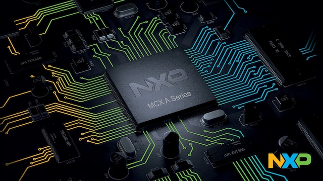


MCX A25是一款必备主流MCU,采用Arm® Cortex® M33内核,主频高达180MHz,配备丰富的串行外设和安全功能
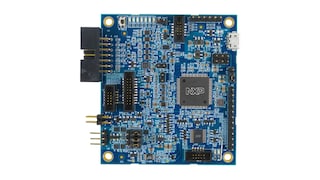
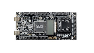
The MCX A34 family of mixed-signal MCUs is purpose-built for motor control applications. These devices use high-performance Arm® Cortex®-M33 cores running up to 180 MHz and deliver strong processing performance. MCX A34 MCUs offer flexible memory configurations from 256KB to 1MB Flash and 64KB to 256KB RAM. MCX A34 MCUs are optimized with the math accelerate unit (MAU) engine and integrate 2x FlexPWM modules with 4 submodules, AOI and up to 4x ADCs. They also feature a rich set of serial peripherals including SmartDMA to support complex control and communication needs.
All devices in the family are supported by the MCUXpresso Developer Experience, which streamlines development and accelerates time-to-market for embedded systems.
| Supported MCUs | Recommended Board | Best Fit For | Key Differentiators |
|---|---|---|---|
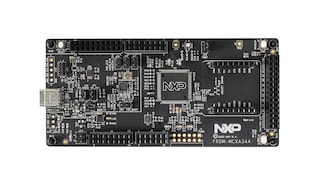
| MCX A343, A344 | FRDM-MCXA344 | Cost-optimized motor control and smart sensing | CAN-FD, MAU, SmartDMA/LCD expansion |
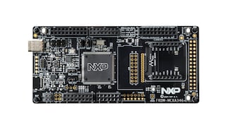
| MCX A345, A346 | FRDM-MCXA346 | Advanced motor control and high-performance real-time designs | 2x FlexPWM, MAU, SmartDMA, CAN-FD |
MCX N94x/54x高度集成的多核MCU,具有片上加速器、智能外设和高级安全功能

MCX A34混合信号,针对电机控制和高性能模拟外设进行了优化
MCX A14x/15x MCU搭载Arm® Cortex® M33内核,提供可扩展的设备选项、低功耗和智能外设
MCX N23x高度集成的MCU,具有片上加速器、智能外设和高级安全功能
LPC552x/S2x:基于Arm® Cortex®-M33的主流微控制器系列
|
|
|
|
|
|
|
|---|---|---|---|---|---|
|
|
|
|
|
|
|
|
|
|
|
|
|
|
|
|
|
|
|
|
|
|
|
|
|
|
|
|
|
|
|
|
|
|
|
|
|
|
|
|
|
|
|
|
|
|
|
|
|
|
|
|
|
|
|
|
|
|
|
|
|
|
|
|
|
|
|
|
|
|
快速参考恩智浦 文档类别
1-10 / 39 文件
紧凑列表
5 硬件
快速参考恩智浦 软件类型.
1-5 / 7 软件文件
可访问其他软件。 查看我们的精选合作伙伴解决方案.
注意: 推荐在电脑端下载软件,体验更佳。
5 培训