

MCX N94x/54x高度集成的多核MCU,具有片上加速器、智能外设和高级安全功能
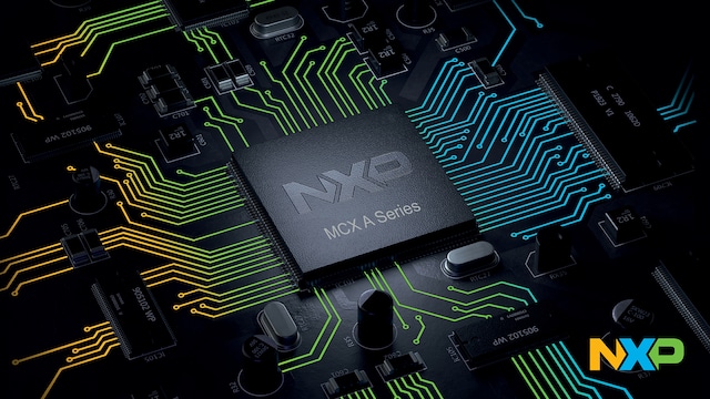
MCX A17系列专为电机控制应用而优化,兼具高性能与高集成度。该系列器件采用Arm® Cortex®-M33内核,工作频率高达180MHz。MCX A17系列包含两个子系列,每个子系列配备4个子模块,并通过AOI逻辑增强,适用于复杂的电机控制。此外,它们还集成了两个ADC、用于高效数据处理的SmartDMA,以及丰富的串行接口(包括I3C、CAN FD、USB与FlexIO)。
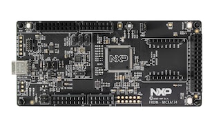
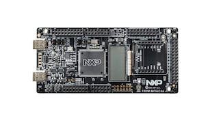
MCX A175和MCX A176提供1MB闪存和256KB RAM。MCX A173和MCX A174提供256KB闪存和64KB RAM。这些特性为开发人员提供了匹配应用需求的灵活性。MCX A17器件配备MCUXpresso Developer Experience支持,提供全面的工具套件,助力简化开发流程并加速产品上市。
| 产品 | 主时钟 | 闪存 | 特性 | 封装 | FRDM板 |
|---|---|---|---|---|---|
| MCXA173 | 180MHz | 128KB | 两个ADC,1个运放,USB,1个CAN | H-PQFN32 LQFP48 LQFP64 LQFP100 | FRDM-MCXA174 |
| MCXA174 | 180MHz | 256KB | 两个ADC,1个运放,USB,1个CAN | H-PQFN32 LQFP48 LQFP64 LQFP100 | FRDM-MCXA174 |
| MCXA175 | 180MHz | 512KB | 两个ADC,1个运放,USB,1个CAN | LQFP64 LQFP100 LQFP144 WFBGA169 | FRDM-MCXA266 |
| MCXA176 | 180MHz | 1024KB | 两个ADC,1个运放,USB,1个CAN | LQFP64 LQFP100 LQFP144 WFBGA169 | FRDM-MCXA266 |
MCX N94x/54x高度集成的多核MCU,具有片上加速器、智能外设和高级安全功能
MCX A14x/15x MCU搭载Arm® Cortex® M33内核,提供可扩展的设备选项、低功耗和智能外设
高效的基于Arm® Cortex®-M33的微控制器产品系列
LPC552x/S2x:基于Arm® Cortex®-M33的主流微控制器系列
|
|
|
|
|
|
|
|---|---|---|---|---|---|
|
|
|
|
|
|
|
|
|
|
|
|
|
|
|
|
|
|
|
|
|
|
|
|
|
|
|
|
|
|
|
|
|
|
|
|
|
|
|
|
|
|
|
|
|
|
|
|
|
|
|
|
|
|
|
|
|
|
|
|
|
|
|
|
|
|
|
|
|
|
快速参考恩智浦 文档类别
1-10 / 15 文件
紧凑列表
4 硬件
快速参考恩智浦 软件类型.
5 软件文件
可访问其他软件。 查看我们的精选合作伙伴解决方案.
注意: 推荐在电脑端下载软件,体验更佳。