
Kinetis KV4x-168 MHz,高性能电机 / 功率变换微控制器(MCU),基于Arm® Cortex®-M4内核
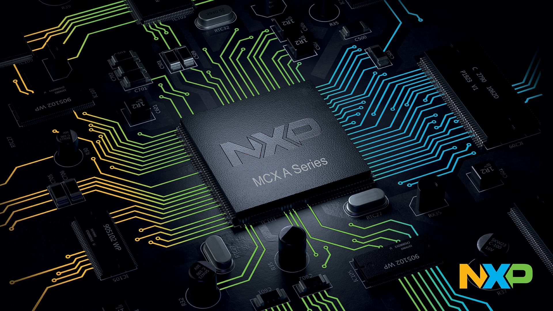
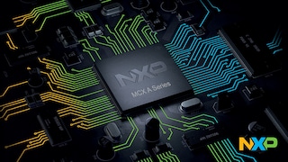
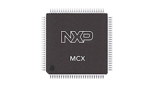
MCX A26: Arm® Cortex®-M33 Mainstream MCU with Rich Serial Peripherals
- This page contains information on a preproduction product. Specifications and information herein are subject to change without notice. For additional information please contact your sales representative.
The MCX A26 family of microcontrollers delivers robust performance with clock speeds up to 240 MHz, featuring up to 1MB of Flash and 256kB of RAM. Engineered for PC accessory applications, these devices offer a comprehensive set of serial peripherals including full-speed USB, dual CAN-FD, I3C and support for 4 x 44-segment LCD displays. FlexIO and SmartDMA enhance flexibility and data handling, while integrated security features ensure reliable operation.
The MCX A265 and A266 are also optimized for motor control, incorporating two FlexPWM modules with four submodules each, AOI logic, and up to two ADCs for precise signal processing.
Development is supported by the MCUXpresso Developer Experience, designed to simplify workflows and accelerate embedded system design.
产品详情
Features
Core Platform
- Arm® Cortex®-M33 240MHz
Processing Accelerators
- SmartDMA co-processor for applications such as parallel camera interface and keypad scanning
Memory
- Single-bank Flash: Up to 1024 kB Flash with error correction code (ECC) (supports one-bit correction and two-bit detection)
- Cache Engine with 8 kB RAM
- Up to 256 kB RAM, including 8 kB shared with cache, configurable as ECC-protected RAM (supports one-bit correction and two-bit detection)
- All RAM can be retained down to Deep Power-down mode
- ROM
Peripherals
- Analog
- 2x 16-bit analog-to-digital (ADC)
- Up to 3.2 Msps in 16-bit mode, and 4 Msps in 12-bit mode
- Up to 43 ADC Input channels total (depending on the package)
- Integrated temperature sensor
- 1 x 12-bit digital-to-analog (DAC)
- Up to 1 Msps
- 2 x High-speed comparators with 8 input pins and 8-bit DAC as internal reference
- 1x low-power analog comparator (LPCMP) is functional down to Deep Power-down mode
- 1x operational amplifier (OPAMP) without programamble gain amplifier (PGA)
- Advanced Motor Control
- Up to 2x FlexPWM each with 4 submodules, providing 16 complementary outputs of pulse width (PWM) (no Nanoedge module)
- Up to 2x Quadrature Encoder/Decoder (eQDC)
- 2x AOI module supports up to 4 output triggers
- Timers
- Includes 5x 32-bit general-purpose asynchronous timers, low-power timer, frequency measurement timer, windowed watchdog timer, wake timer, microtick timer (UTICK), OS event timer, and RTC timer (no external 32 kHz input required)
- Low power timer
- Frequency measurement timer
- Windowed watchdog timer
- Wake timer
- Microtick timer (UTICK)
- OS event timer
- Real-time clock (RTC) timer without external 32 kHz input
- Communication Interfaces for Connectivity
- 2x low-power serial peripheral interface (LPSPI), 4x low-power inter-integrated circuit (LPI2C), 6x ow-power universal asynchronous receiver-transmitter (LPUART)
- 1x Improved Inter-Integrated Circuit (I3C)
- USB Full-speed (Device/Host) with on-chip full-speed physical layer (FS PHY)
- 1x FlexCAN with flexible data-rate (FD)
- 2x FlexCAN with FD
- Human-machine interface (HMI)
- FlexIO
- Segment LCD supports 4x44
Security
- EdgeLock Accelerator
- Public Key Cryptography (PKC), supports ECC and RSA encryption and decryption
- Secure Generic Interface (SGI), provides AES256, SHA-2 and key generation/derivation
- Secure key store with key usage policies (protection of platform integrity, manufacturing and applications keys)
- 128-bit niversal unique identifier (UUID) per device in accordance with IETF's RFC4122 version 5 specification
- Device life cycle management
- Flash read, write and execute permission protected by memory boundary controller (MBC) and lockable
- Implicit-protected Flash Region (IFR)
- Security Monitoring
- Code watchdog for code flow integrity checking
- Glitch attack resistant keyed access (Glikey) to security sensitive registers
- 6x Passive anti tamper detect
- Secure Installer for secure-manufacturing and IP theft protection in untrusted factory
Packaging
- WFBGA169 7x7mm, LQFP144 20x20mm, LQFP100 14x14mm, LQFP64 10x10mm
MCUXpresso Developer Experience
- MCUXpresso ecosystem support
- Selection of ntegrated development environments (IDE) choices
- Pin, clock, peripheral, security and memory config tools
- Security programming and provisioning tools
- Software development kit (SDK)
- Zephyr real-time operating system (RTOS) support
相关产品

MCX A17 Essential MCU Arm® Cortex® M33 with 180 MHz and Rich Serial Peripherals
MCX A18 Essential Mainstream MCU Arm® Cortex® M33 with 240MHz and Rich Serial Peripherals
MCX A14x/15x MCU搭载Arm® Cortex® M33内核,提供可扩展的设备选项、低功耗和智能外设
高效的基于Arm® Cortex®-M33的微控制器产品系列
MCX N94x/54x高度集成的多核MCU,具有片上加速器、智能外设和高级安全功能
LPC552x/S2x:基于Arm® Cortex®-M33的主流微控制器系列
设计资源

软件
快速参考恩智浦 软件类型.
4 软件文件
-
BSP及设备驱动
MCUXpresso配置工具 - 引脚、时钟、外设
-
开发IDE和生成工具
MCUXpresso集成开发环境(IDE)
-
可访问其他软件。 查看我们的精选合作伙伴解决方案.
-
开发IDE和生成工具
MCUXpresso for Visual Studio Code
注意: 推荐在电脑端下载软件,体验更佳。