FRDM-A-S32K358通用开发板快速入门
1. 开箱即用
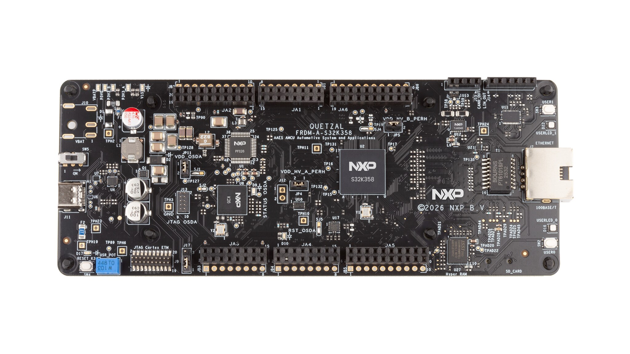
恩智浦FRDM-A-S32K358搭载两个锁步模式配置的Arm® Cortex®-M7内核,以及一个主频为240MHz的Arm Cortex-M7内核,配备ASIL-D安全硬件、8MB闪存、硬件安全引擎B (HSE B),支持无线(OTA)更新,具有先进的连接、浮点单元(FPU)及低功耗特性。

1.1 套件内含物/装箱单
该套件内含物包括:
- 完成组装和测试的开发板,放在防静电袋中
- 快速入门指南
- USB Type-C线
1.2 最低系统要求
要完成板评估,需要一台安装了Windows操作系统的PC。为获得最佳效果,PC应支持USB接口,并运行Windows 7、10或11操作系统。
2. 获取软件
2.1 板特性
- 恩智浦系统基础芯片(SBC) FS26
- USB-Type C端口
- 通过板载K26微控制器(MCU)实现的OpenSDA调试
- 一个20引脚JTAG连接器
- 两个按钮
- 1个电位计
- 两个RGB LED
- 一个64MB HyperRAM存储器
- 1个SD卡连接器
2.2 板说明
恩智浦FRDM-A-S32K358搭载两个配置为锁步模式的Arm Cortex-M7内核,以及一个主频为240MHz的Arm Cortex-M7内核。该板还配备ASIL-D安全硬件、8MB闪存、硬件安全引擎B (HSE B),支持无线(OTA)更新,具有先进的连接、浮点单元(FPU)及低功耗特性。它搭载了恩智浦SBC FS26,可为安全关键型应用提供+5.0V和+3.3V电源轨。FRDM-A-S32K358集成了恩智浦PTN5110 USB PD物理层(PHY),可通过单个USB Type-C®端口实现高压、大电流供电与数据传输。
2.3 板组件
FRDM-A-S32K358配备集成的OpenSDA调试接口、板载K26微控制器(MCU)以及USB Type-C端口。该端口支持多种调试接口,包括20引脚JTAG连接器,便于外部工具接入并实现便捷连接。
其他特性包括两个按钮、一个电位计、两个RGB LED、一个64MB HyperRAM存储器,以及用于原型制作的选定MCU输入/输出(I/O)引脚。
板载RJ45连接器支持以太网100BASE/T,TJA1043和TJA1425收发器则分别支持5Mbit/s CAN FD和2.1/SAEJ2602 LIN PHY,共同确保汽车与工业应用的可靠通信。板载车规级NXP FXLS8961加速度传感器和NXP P3T1750温度传感器提供实时环境反馈。
2.4 安装软件
- 通过以下链接访问软件包:FRDM Automotive套件
- 点击“生成”进行下载
- 运行恩智浦多重安装程序
- 通过已创建的桌面快捷方式启动S32 Design Studio for S32 Platform 3.6.5
通过勾选"下载后启动可执行文件"(Launch executable after download)和"无需任何交互的安装与配置"(Installation and configuration without any interaction)选项,FRDM软件包及其所有可用组件将被一并安装。
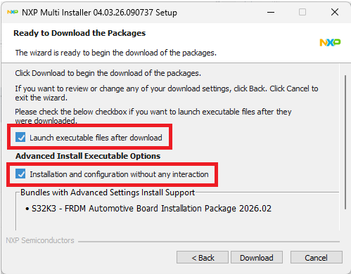
所有软件及工具现已自动完成安装与配置。
3. 连接
3.1 连接
FRDM-A-S32K358是一款基于S32K3X8EVB-Q289的快速原型制作板。该板并非为最终量产用途设计,因此采用通过USB PD连接至FS26 SBC的主电源选项。该配置的详细信息见表1。更多详情请参见UM12541《FRDM-A-S32K358开发板用户手册》。
| 模式 | 支持的最大电压/电流 | 说明 |
|---|---|---|
| 通过USB Type-C连接器的PD供电 | 典型输入:+5V/3A 支持的最大电压/电流:+20V/3A |
默认情况下,FRDM-A-S32K358通过J11 USB Type-C连接器供电。建议使用随附的USB Type-C线,或任何支持USB Power PD的线缆,以确保板的全部功能正常运行。使用其他线缆可能导致电流供应受限,并降低性能。要正常为板供电,需要使用支持USB-C PD的电源,例如USB-C PD充电器或支持PD协议的笔记本电脑。虽然大多数现代笔记本电脑都支持USB PD,但使用前请确认您的设备是否具备此功能。使用其他线缆可能导致电流供应受限,并降低性能。 FRDM-A-S32K358支持高达20V的输入电压。但根据FS26 SBC的建议,最佳工作电压范围为9V、12V或15V,且电流至少为1A。要实现上述电压和电流等级,需要USB PD电源与PD PHY (PTN5110)之间进行正确的协商。有关如何在S32K358上实现此协商的指导,请咨询当地的恩智浦现场应用工程师(FAE),或访问恩智浦应用代码中心网站获取相关代码。 FS26负责电源管理,将VBAT输入转换为S32K358各电源域所需的稳定电压轨。 |
| 通过圆柱形连接器正常运行 | +12V/2A | FRDM-A-S32K358的第二种供电方式是通过圆柱形插孔连接器(J10)连接外部+12V/2A电源。该选项默认被禁用,需手动焊接以下组件方可启用:
J10供电,作为USB Type-C PD供电的替代方案。 |
4. 构建、运行
4.1 构建、运行
| 步骤顺序 | 说明 |
|---|---|
| 1. | 将USB Type-C线连接至J11连接器,给板上电。 |
| 2. | 要给板上电,将开关SW5的默认位置更改为2-3设置。 |
| 3. | 确认板上的所有电源LED指示灯均已亮起。 |
| 接口 | FRDM-A-S32K358 | 参考/信号 | 默认配置 | 说明/注释 |
|---|---|---|---|---|
| MCU | ● | U2 | S32K358 MCU | S32K358 Arm Cortex-M7,240MHz,8MB闪存,CAN FD,HSE B安全,289 MAPBGA |
| 外设供电跳线 | ● | JP4 |
1-2 | 选择外设输入供电 |
| ● | JP5 |
1-2 | ||
| MCU电源 | ● | VDD_HV_A | +3.3V | +3.3V参考电压由FS26 LDO1稳压器提供,并路由至S32K358的VDD_HV_A电源域(通过R806 [FS26_VTRK1],可在VDD_HV_A提供5V ) |
| ● | VDD_HV_B | +3.3V | +3.3V参考电压由FS26 LDO2稳压器提供,并路由至S32K358的VDD_HV_B电源域 | |
| ● | V15 |
+1.5V | +1.5V参考电压由FS26 VCORE稳压器提供,并路由至S32K358的V15核心电源域。( V15电源轨也可通过S32K358控制的外部晶体管供电;要启用此配置,需安装晶体管Q5及相关电路,并正确路由焊锡跳线SJ4) |
|
| ● | V11 |
+1.1V | 核心逻辑电源,在内部生成 | |
| 板载调试OpenSDA | ● | J11 |
已启用 | 默认情况下,USB Type-C连接器被配置为主要调试接口 |
| ● | JP11 |
1-2 | JP11默认路由,用于使能OpenSDA电压 |
|
| ● | PTA15–LPUART6_RX | 已启用 | 用于PC串行通信。 | |
| ● | PTA16–LPUART6_TX | 已启用 | ||
| JTAG | ● | J9 | 已禁用 | S32K358 MCU的JTAG接口可通过20引脚Arm Cortex Debug + plus ETM连接器进行访问(要启用该接口,必须移除跳线JP11 [OpenSDA voltage]) |
| USB Type-C PD | ● | J11 |
已启用 | 默认情况下,USB Type-C连接器被配置为USB PD的主接口(可使用随附线缆或任何支持PD协议的USB-C线为板供电) |
| ● | SW5 | 1-2 | 如果连接至板的电源支持USB-C通信,SW5开关将根据CC线路的连接或断开状态控制板的通断;默认情况下,板为断电状态 | |
| ● | VBUS_IN | +5.0V | 默认情况下,VBUS_IN线路电压为+5.0V (如需通过USB Power PD请求更高电压,须通过I²C接口与PTN5110控制器发起有效的电压协商;板最高支持20V,建议典型工作电压为9V、12V或15V) | |
| ● | PTC7–LPI2C_ SCL | 已启用 | PTC7 LPI2C串行时钟(SCL)默认路由至PTN5110和NX20P3483 | |
| ● | PTC6–LPI2C_ SDA | 已启用 | PTC6 LPI2C串行数据(SDA)默认路由至PTN5110和NX20P3483 | |
| 以太网 | ● | U14 | 已启用 | 默认情况下,以太网接口以RMII模式路由至KSZ8091RNDIA 100BASE-T以太网PHY,并连接至RJ45连接器(J7) |
| QUAD LIN接口 | ● | J14 |
J14-2 LIN1 |
由LPUART9配置,电压电平被限制为VSUP电压,当VBAT上为5V时,典型值为11.5V |
| ● | J14-3 LIN2 |
由LPUART9配置,电压电平被限制为VSUP电压,当VBAT上为5V时,典型值为11.5V | ||
| ● | J14-4 LIN3 |
由LPUART9配置,电压电平被限制为VSUP电压,当VBAT上为5V时,典型值为11.5V | ||
| ● | J14-5 LIN4 |
由LPUART9配置,电压电平被限制为VSUP电压,当VBAT上为5V时,典型值为11.5V | ||
| 控制器局域网(CAN)接口 | ● | J15 |
J15-1–CANHJ15-2–CANL |
S32K358通过CAN0_RX和CAN0_TX信号线连接至TJA1043 CAN收发器——电压电平被限制为VSUP电压(当VBAT上为5V时,典型值为11.5V) |
| 用户RGB LED | ● | D16 | PTG29 | 红色[高电平有效] |
| ● | PTG30 | 绿色[高电平有效] | ||
| ● | PTG31 | 蓝色[高电平有效] | ||
| ● | D22 | PTF21 | 红色[高电平有效] | |
| ● | PTF22 | 绿色[高电平有效] | ||
| ● | PTF23 | 蓝色[高电平有效] | ||
| 用户按钮 | ● | SW3 | PTH3 | 带WKUP15 |
| ● | SW2 | PTH1 | 带WKUP0 | |
| ● | SW3 | DNP PTC31 | 带WKUP49 | |
| 模数转换器电位计 | ● | R370 | PTA17 | 带ADC2_S19 |
| ● | R370 | DNP PTC23 | 带ADC2_S23 | |
| HyperRAM存储器 | ● | U27 | 已启用 | ISSI IS66WVH8M8FBLLPSRAM——伪静态随机存取存储器(SRAM)——存储器64Mb,166MHz,24 TFBGA封装 |
| SD卡连接器 | ● | J16 | 已启用 | S32K358通过SD主机控制器(uSDHC)线路连接至SD卡连接器。 |
| 加速度传感器 | ● | FXLS8961AF | 已启用 | ±2g/±4g/±8g/±16g,低功耗12位数字加速度传感器(具备超低功耗运动唤醒功能,符合AEC-Q100标准,PTC7与PTC6 I²C线路默认路由) |
| 温度传感器 | ● | P3T1750 | 已启用 | 12位温度-数字转换器,测量范围-40°C至+125°C,精度为±1°C,数字温度传感器。符合AEC-Q900标准。PTC7与PTC6 I²C线路默认路由 |
| ARDUINO接头 | ● | - | - | 该板兼容ARDUINO UNO、DEVKIT-MOTORGD和DEVKIT-COMM板。(具体引脚布线详情请参见原理图) |
设计资源
支持
培训
论坛
访问恩智浦的技术社区网站,与其他工程师交流,获取如何使用FRDM-A-S32K358开发板进行产品设计的专业建议。