Getting Started with the FRDM Automotive S32K356 Development Board for General Purpose

上次修改时间: Jun 5, 2026支持 FRDM-A-S32K356开发板

本文档内容

  • 1

    Out of the Box
  • 2

    Get Software
  • 3

    Plug It In

1. Out of the Box

The NXP FRDM-A-S32K356 features dual Arm® Cortex®-M7 cores configured in lockstep mode and along with a single Arm Cortex-M7 core running at 240 MHz, ASIL-D safety hardware, 8 MB flash, Hardware Security Engine B (HSE B), over-the-air (OTA) support, advanced connectivity, floating-point unit (FPU) and low power.

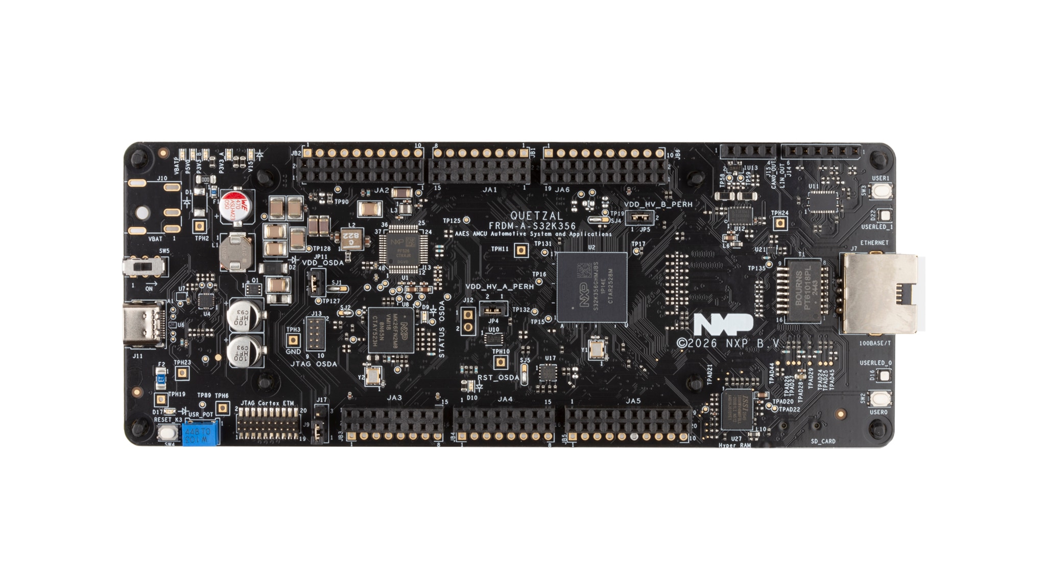
FRDM-A-S32K356 Top View

FRDM-A-S32K356 Top View

FRDM Automotive S32K356 Development Board

FRDM Automotive S32K356 Development Board

1.1 Kit Contents/Packing List

The Kit Contents includes:

  • Assembled and tested development board in an antistatic bag
  • Quick Start Guide
  • USB Type-C cable

1.2 Minimum System Requirements

For board evaluation, you will need a Windows PC. For best results, the PC should be USB-enabled and running on either Windows 7, 10 or 11.

1.3 Software

You will also need to install software for board evaluation. All listed software is available on the development board's information page at FRDM-A-S32K356 development board's information page or from the Automotive Package Manager.

2. Get Software

2.1 Board Features

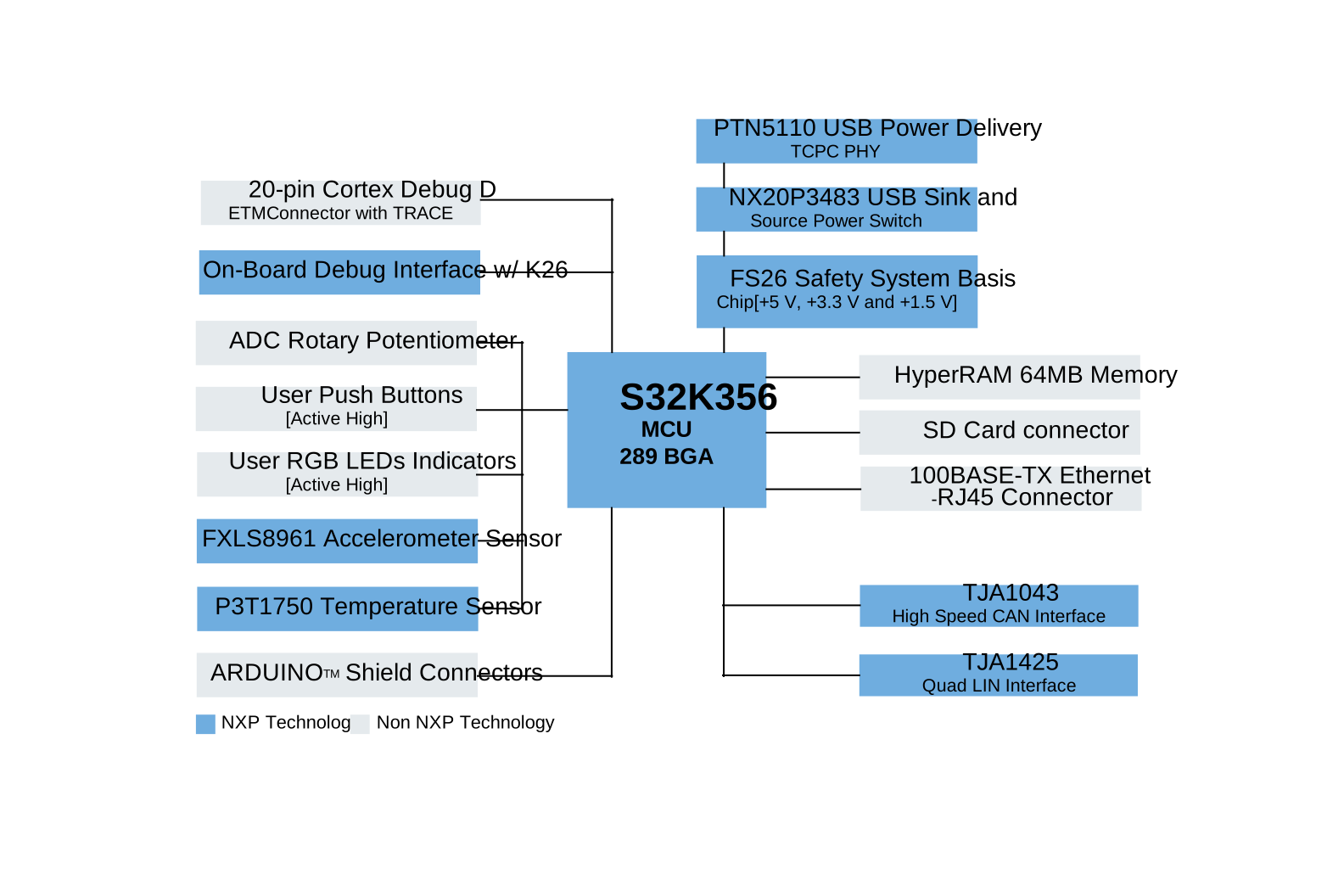
  • NXP system basis chip (SBC) FS26
  • USB Type-C C port
  • Open Serial and Debug Adapter (OpenSDA) debug with the onboard K26 microcontroller (MCU)
  • One 20-pin Joint Test Action Group (JTAG) connector
  • Two push buttons
  • One potentiometer
  • Two RGB LED
  • One 64 MB Hyper-RAM memory
  • One SD card connector

2.2 Board Description

The NXP FRDM-A-S32K356 features dual Arm Cortex-M7 cores configured in lockstep mode along with a single Arm Cortex-M7 running at 40 MHz. The board also includes ASIL-D safety hardware, 6 MB flash, Hardware Security Engine B (HSE B), over-the-air (OTA) support, advanced connectivity floating-point unit (FPU) and low-power low-power. It includes the NXP SBC FS26, which provides +5.0 V and +3.3 V power rails for safety-critical applications. The FRDM-A-S32K356 integrates the NXP PTN5110 USB Power Delivery (PD) physical layer (PHY), enabling high-voltage, high-current power and data through a single USB Type-C port.

2.3 Board Components

The FRDM-A-S32K356 is equipped with an integrated OpenSDA debug, an onboard K26 microcontroller unit (MCU) and a USB Type-C port that supports multiple debug interfaces, including a 20-pin JTAG connector for external tools and convenient connectivity.

Additional features include two push buttons, a potentiometer, two RGB LEDs, a 64 MB Hyper-RAM memory and access to selected MCU input/output (I/O) pins for prototyping.

The inclusion of Ethernet 100BASE/T with the RJ45 connector, Controller Area Network Flexible Data-Rate (CAN FD) at 5 Mbit/s, and Local Interconnect Network (LIN) at 2.1/SAEJ2602 PHYs, powered by the TJA1043 and TJA1425 transceivers—ensure reliable communication for automotive and industrial applications. The onboard automotive-grade NXP FXLS8961 accelerometer and NXP P3T1750 temperature sensor provide real-time environmental feedback.

2.4 Install Software

  1. Go to the software bundle using the following link FRDM Automotive Bundle
  2. Click Generate to download
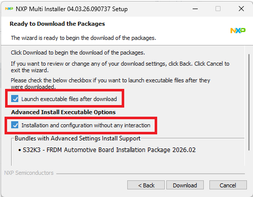
  3. Run the NXP Multi Installer
  4. By selecting “Launch executable after download” and “Installation and configuration without any interaction” the FRDM Bundle will be installed alongside all its available components.

    NXP Multi Installer

    NXP Multi Installer

    All the Software and Tools are now installed and configured automatically.

  5. Launch S32 Design Studio for S32 Platform 3.6.5 from the shortcut that has been created on your desktop

3. Plug It In

3.1 Plug It In

The FRDM-A-S32K356 is a rapid prototyping board based on the S32K3X8EVB-Q289. As it is not intended for final production use, the board includes a primary power-supply option through USB PD connected to the FS26 SBC. Details of this configuration are provided in Table 1. See UM12542, FRDM-A-S32K356 Development Board User Manual for further details.

Mode Max Voltage / Current Supported Description
PD with USB Type-C Connector Typical Input: +5 V/3 A
Maximum Supported: Up to +20 V/3 A
Note: Actual current depends on the capabilities of the connected USB Type-C power source
By default, the FRDM-A-S32K356 is powered via the J11 USB Type-C connector. It is recommended to use the USB Type-C cable included in the box, or another cable that supports USB PD, to ensure full functionality of the board. Using an alternative cable may result in limited current supply and reduced performance.
To power the board properly, a USB-C PD–compatible power source is needed, such as a USB-C PD charger or a laptop with PD support. While most modern laptops support USB PD, verify your device’s capabilities before use. Using an alternative cable may result in limited current supply and reduced performance.
The FRDM-A-S32K356 supports input voltages up to 20 V. However, based on FS26 SBC recommendations, it is ideal to operate within 9 V, 12 V or 15 V ranges with at least 1 A. Achieving these voltages and current levels requires proper negotiation/communication between the USB PD source and the PD PHY (PTN5110). For guidance on implementing this negotiation with the S32K356, consult your local NXP field application engineer (FAE) or the code available in the NXP Application Code Hub (ACH) website.
The FS26 manages power regulation by converting the VBAT input into stable voltage rails required by the S32K356’s power domains.
Note: If a USB Type-A-to-USB Type-C cable is used to power the board, the integrated switch will not power off the board due to the lack of the cable control lines for power delivery. To avoid this issue, always use the cable provided.
The second power supply method for the FRDM-A-S32K356 involves connecting an external +12 V/2 A power source to the barrel jack connector (J10).
Operation with Barrel Connector +12 V/2 A This option is disabled by default and requires manual soldering of the following components to enable it: J10: Barrel connector
C1, C9: Input capacitors
D1: Protection diode
Once these components are populated, the board can be powered through J10 as an alternative to USB Type-C PD.
Step sequence Description
1. Connect the USB Type-C cable to the J11 connector to supply power to the board
2. To power on the board, change the position of switch SW5 to setting 2–3
3. Verify that all power indicator LEDs on the board are illuminated
Interface FRDM-A-S32K356 Reference / Signal Default configuration Description / Comment
MCU U2 S32K356 MCU S32K356 Arm Cortex-M7, 240 MHz, 8 MB flash, CAN FD, HSE B security, 289 molded array process ball grid array (MAPBGA)
Supply Peripheral Jumpers JP4 1 - 2 Selects the peripherals input supply
JP5 1 - 2
MCU Power Supply VDD_HV_A +3.3 V The reference voltage of +3.3 V is supplied by the FS26 low-dropout 1 (LDO1) regulator and routed to the VDD_HV_A power domain of the S32K356 (5 V can be supplied on VDD_HV_A with R806 [FS26_VTRK1])
VDD_HV_B +3.3 V The reference voltage of +3.3 V is supplied by the FS26 LDO2 regulator and routed to the VDD_HV_B power domain of the S32K356.
V15 +1.5 V The reference voltage of +1.5 V is supplied by the FS26 Core voltage (VCORE) regulator and routed to the V15 core power domain of the S32K356. (Optionally, the V15 rail can be powered through an external transistor controlled by the S32K358, so to enable this configuration, transistor Q5 and circuitry must be populated and solder jumper SJ4 must be properly routed)
V11 +1.1 V Core logic supply internally generated
On-Board Debug OpenSDA J11 Enabled The USB Type-C connector is configured by default as the primary interface for debugging
JP11 1 - 2 JP11 is routed as default enabling the OpenSDA voltage
PTA15 – LPUART6_RX Enabled For PC serial communication
PTA16 – LPUART6_ TX Enabled
JTAG J9 Disabled The JTAG interface of the S32K356 MCU is accessible via a 20-pin Cortex Debug plus Embedded Trace Macrocell (ETM) connector. (to enable this interface, jumper JP11 [OpenSDA voltage] must be removed)
USB Type-C PD J11 Enabled By default, the USB Type-C connector is configured as the primary interface for USB PD (the included cable—or any USB Type-C cable that supports PD—can be used to power the board)
SW5 1 - 2 If the power source connected to the board supports USB Type-C communication, switch SW5 turns the board on or off based on the connection or disconnection of the CC lines, so by default the board is off.
VBUS_IN +5.0 V By default, the voltage on the VBUS_IN line is +5.0 V (to request a higher voltage via USB PD, a valid voltage negotiation must be initiated through the inter-integrated circuit (I²C) interface with the PTN5110 controller and the board supports up to 20 V with 9 V, 12 V or 15 V recommended for typical operation)
PTC7–LPI2C_SCL Enabled PTC7 LPI2C serial clock (SCL) is routed by default to the PTN5110 and NX20P3483
PTC6–LPI2C_SDA Enabled PTC6 LPI2C serial data (SDA) is routed by default to the PTN5110 and NX20P3483
Ethernet U14 Enabled By default, the Ethernet interface is routed in RMII mode to the KSZ8091RNDIA 100BASE-T Ethernet PHY, which is connected to the RJ45 connector (J7)
QUAD Local Interconnect Network (LIN) Interface J14 J14-2 LIN1 Configured by LPUART9, voltage levels are limited to VSUP voltage (typical 11.5 V when 5 V is on VBAT)
J14-3 LIN2 Configured by LPUART12 voltage levels are limited to VSUP voltage (typical 11.5 V when 5 V is on VBAT)
J14-4 LIN3 Configured by LPUART4 voltage levels are limited to VSUP voltage (typical 11.5 V when 5 V is on VBAT)
J14-5 LIN4 Configured by LPUART8 voltage levels are limited to VSUP voltage (typical 11.5 V when 5 V is on VBAT)
Controller Area Network (CAN) Interface J15 J15-1–CANH The S32K356 is connected to a TJA1043 CAN transceiver via the CAN0_RX and CAN0_TX signal lines—voltage levels are limited to VSUP voltage (typical 11.5 V when 5 V is on VBAT)
J15-2–CANL
User RGB LED D16 PTG29 Red [Active High]
PTG30 Green [Active High]
PTG31 Blue [Active High]
D22 PTF21 Red [Active High]
PTF22 Green [Active High]
PTF23 Blue [Active High]
User Push Button SW3 PTH3 With WKUP15
SW2 PTH1 With WKUP0
SW3 DNP PTC31 With WKUP49
Analog-to-Digital Converter Potentiometer R370 PTA17 With ADC2_S19
R370 DNP PTC23 With ADC2_S23
HyperRAM Memory U27 Enabled IS66WVH8M8FBLLPSRAM—Pseudo static random-access memory (SRAM)—Memory Integrated Circuit (IC) 64Mbit HyperBus 166 MHz 24-thin fine-pitch ball grid array (TFBGA)
SD Card Connector J16 Enabled The S32K356 is connected to an SD Card Connector with the secure digital host controller (uSDHC) lines
Acceleration Sensor FXLS8961AF Enabled ±2 g/±4 g/±8 g/±16 g, Low-power 12-bit digital accelerometer (with ultra-low power wake up on motion, AEC-Q100, PTC7, PTC6 I²C lines are routed by default)
Temperature Sensor P3T1750 Enabled Temperature-to-digital 12-Bit converter from -40 °C to +125 °C range—1 °C accuracy, digital temperature sensor, AEC-Q900, PTC7, PTC6 I²C lines are routed by default
ARDUINO Headers - - This board incorporates compatibility with ARDUINO UNO, DEVKIT-MOTORGD and DEVKIT-COMM boards (consult the schematic for more details in the routed pins)

Support

Forums

Connect with other engineers and get expert advice on designing with the FRDM-A-S32K344 Development Board using our community sites.