As I3C adoption accelerates across next-generation computing and embedded systems, NXP recognized a critical
infrastructure gap: designers needed a purpose-built buffer that could preserve I3C performance while supporting
voltage translation, larger bus capacitance, and longer PCB traces. The new P3B1602DP addresses that need with a 2-bit
I3C bus buffer supporting up to 12.5 MHz SDR and DDR operation, voltages as low as 0.72 V, and capacitive loads up to
100 pF.
Interview with Bob Gee on the NXP P3B1602DP
Q1: NXP appears to be first-to-market with an I3C bus buffer. Why did NXP decide to develop this product?
Bob Gee: We saw a clear need emerging as the industry transitions from I²C to I3C. New processors,
SoCs, application processors, MCUs, and system controllers are increasingly adopting I3C because it provides
significantly higher performance, greater efficiency, and better system scalability than legacy interfaces.
As adoption increased, system designers began running into practical challenges. I3C buses are optimized for higher
speeds and generally lower bus capacitance, but many real-world systems require longer PCB traces, connectors,
multiple board-to-board links, or voltage translation between devices operating at different supply rails.
What was missing from the market was a dedicated buffer designed specifically for I3C. NXP recognized that gap early
and developed the P3B1602DP to help customers extend I3C buses without sacrificing the performance advantages that
motivated their migration to I3C in the first place.
The result is a device that combines buffering, bidirectional level translation, automatic direction sensing, and
support for larger capacitive loads, making I3C easier to deploy in demanding system architectures.
Enable next-generation I3C architecture. Learn more about the P3B1602DP and download the datasheet.
Q2: Modern processors continue to operate at lower voltages. How does the P3B1602DP address this challenge?
Bob Gee: One of the key strengths of the P3B1602DP is its exceptionally wide and low voltage
operating range. Port A supports supply voltages from 0.72 V to 1.98 V, while Port B supports
1.08 V to 3.63 V, allowing seamless communication between next-generation low-voltage controllers and
higher-voltage peripheral devices.
This is particularly important in modern AI servers, data center accelerators, networking equipment, robotics
platforms, and telecom infrastructure. The latest SoCs and application processors often operate at core voltages
around 0.8 V to 1.2 V, while attached sensors, power devices, DDR memory, and management ICs may operate at higher
voltages.
The P3B1602DP eliminates the need for designers to compromise between performance and interoperability. It allows
customers to leverage the benefits of low-voltage silicon while maintaining compatibility across mixed-voltage systems
through automatic bidirectional voltage-level translation.
 Support seamless I3C communication across today's mixed-voltage server and embedded
systems.
Q3: I3C is known for its speed. How does the P3B1602DP help maintain signal integrity at high bandwidths?
Bob Gee: The promise of I3C is high bandwidth. The P3B1602DP fully supports I3C operation with data
rates up to 12.5 MHz SDR and DDR, while also supporting legacy I²C and SMBus interfaces.
However, high-speed operation alone is not enough. System designers frequently need to drive larger loads than a
typical I3C bus was originally intended to support. That's where the P3B1602DP stands out.
The device is designed to support up to 100 pF capacitive loading, which is double the allowable
capacitance for an I3C bus. It also incorporates a longer one-shot accelerator pulse, specifically engineered to drive
larger capacitive loads and compensate for longer signal propagation paths.
In practical terms, this means customers can support:
- Longer PCB traces
- Larger backplanes
- Board-to-board interconnects
- Greater round-trip signal delays
- Higher capacitive loading
Without giving up the performance advantages of I3C. The datasheet specifically notes support for larger capacitive
loads, longer round-trip delays, and PCB traces up to approximately 40 inches.
For applications such as AI servers, accelerator cards, telecom line cards, industrial robotics, and advanced embedded
computing, this capability can significantly simplify system-level design while maintaining reliable high-speed
communication.
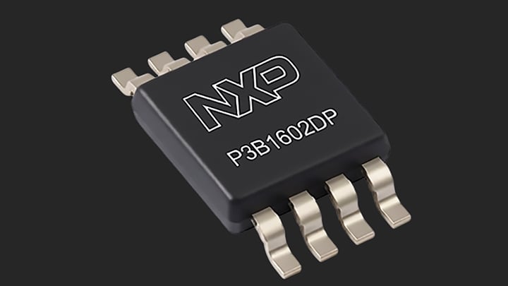 NXP's P3B1602DP dedicated I3C bus buffer for high-speed, long-reach system designs.
Q4: Why is it important to use an industry-standard TSSOP8 package and pinout?
Bob Gee: Ease of adoption was a major design goal. Engineers don't just evaluate electrical
performance; they also consider how quickly a device can be integrated into existing hardware platforms.
The P3B1602DP is offered in an industry-standard TSSOP8 package with a familiar pinout and a compact
3 mm × 3 mm footprint. This allows customers to adopt the device with minimal layout disruption and often reuse
existing design practices and manufacturing processes.
Just as importantly, the device is specified across a-40°C to +125°C temperature range, making it suitable for
environments that require industrial and infrastructure-grade robustness.
This combination of standard packaging, broad voltage support, high-speed I3C capability, and extended temperature
operation make it an attractive solution for:
- AI data centers
- Enterprise servers
- Telecom infrastructure
- Industrial automation
- Robotics platforms
- Edge computing equipment
Ultimately, we wanted customers to benefit from cutting-edge I3C performance without introducing unnecessary adoption
barriers, and the standard TSSOP8 footprint helps accomplish exactly that.
Closing Thoughts
Bob Gee: The P3B1602DP demonstrates NXP's commitment to enabling the next generation of system
architecture. By being first to address the emerging need for an I3C-specific buffer, NXP has created a solution that
combines ultra-low-voltage support, high-speed I3C performance up to 12.5 MHz, robust 100 pF drive capability for
longer signal paths, and an industry-standard TSSOP8 package that simplifies implementation across data center,
server, robotics, industrial, and telecom applications.