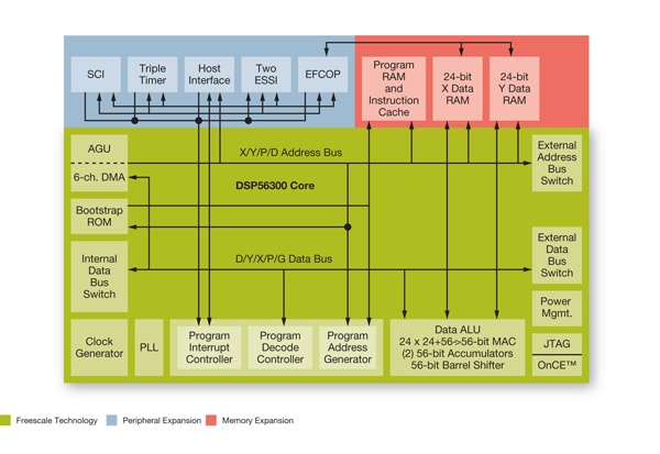
24-bit General Embedded DSP

DSP56311

查看产品图片

产品详情

选择区域:

框图

DSP56311 Block Diagram

特征

  • 150 MMACS (300 MIPS using the EFCOP in filtering applications) with a 150 MHz clock at 1.8 volts
  • Object code compatible with the DSP56000 core with highly parallel instruction set
  • Data arithmetic logic unit (data ALU) with fully pipelined 24 x 24-bit parallel
  • Multiplier-accumulator (MAC), 56-bit parallel barrel shifter (fast shift and normalization, bit stream generation and parsing), conditional ALU instructions and 24-bit or 16-bit arithmetic support under software control
  • Program control unit (PCU) with position-independent code (PIC) support, addressing modes optimized for DSP applications (including immediate offsets), on-chip instruction cache controller, on-chip memory-expandable hardware stack, nested hardware DO loops and fast auto-return interrupts
  • Direct memory access (DMA) with six DMA channels supporting internal and external accesses; one-, two-, and three-dimensional transfers (including circular buffering); end-of-block- transfer interrupts; and triggering from interrupt lines and all peripherals
  • Phase-lock loop (PLL) allows change of low-power divide factor (DF) without loss of lock
  • Hardware debugging support including on-chip emulation (OnCE) module, JTAG test access port
  • 128K on-chip RAM total program RAM, instruction cache, X data RAM and Y data RAM sizes are programmable:
    Program
    RAM Size
    Instruction
    Cache Size
    X Data
    RAM Size*
    Y Data
    RAM Size*
    32 K x 24-bit
    0
    48 K x 24-bit
    48 K x 24-bit
    31 K x 24-bit
    1024 x 24-bit
    48 K x 24-bit
    48 K x 24-bit
    96 K x 24-bit
    0
    16 K x 24-bit
    16 K x 24-bit
    95 K x 24-bit
    1024 x 24-bit
    1 6 K x 24-bit
    16 K x 2 4-bit
    80 K x 24-bit
    0
    24 K x 24-bit
    24 K x 24-bit
    79 K x 24-bit
    1024 x 24-bit
    24 K x 24-bit
    24 K x 24-bit
    64 K x 24-bit
    0
    32 K x 24-bit
    32 K x 24-bit
    63 K x 24-bit
    1024 x 24-bit
    32 K x 24-bit
    32 K x 24-bit
    48 K x 24-bit
    0
    40 K x 24-bit
    40 K x 24-bit
    47 K x 24-bit
    1024 x 24-bit
    40 K x 24-bit
    40 K x 24-bit
    * Includes 10 K x 24-bit shared memory (i.e., memory shared by the core and the EFCOP).
  • 192 x 24-bit bootstrap ROM
  • Data memory expansion to two 256 K x 24-bit word memory spaces using standard external address lines
  • Program memory expansion to one 256 K x 24-bit word memory space using standard external address lines
  • External memory expansion port
  • Chip select logic for glueless interface to SRAMs
  • 3.3-volt I/O interface enhanced 8-bit parallel host interface (HI08) supports a variety of buses (for example, ISA) and provides glueless connection to a number of industry-standard microcomputers, microprocessors and DSPs
  • Two enhanced synchronous serial interfaces (ESSI0 and ESSI1), each with one receiver and three transmitters
  • Serial communications interface (SCI) with baud-rate generator
  • Triple timer module
  • Up to 34 programmable general-purpose I/O (GPIO) signals, depending on which peripherals are enabled
  • Enhanced filter coprocessor (EFCOP) running in parallel with the core
  • Very low-power CMOS design
  • Wait and stop low-power standby modes
  • Fully static design specified to operate down to 0 Hz (DC)
  • Optimized power management circuitry (instruction-dependent, peripheral-dependent and mode-dependent)

部件编号包含: DSP56311VF150, DSP56311VL150.

文档

快速参考 文档类别.

1-5 / 62 文件

展开

设计资源

选择区域:

设计文件

3 设计文件

支持

您需要什么帮助?