开始使用S32K389EVB-Q437进行开发
本文档内容
-
开箱即用
-
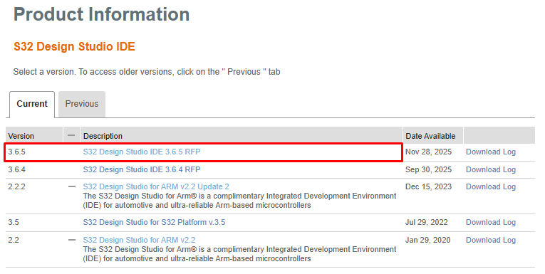
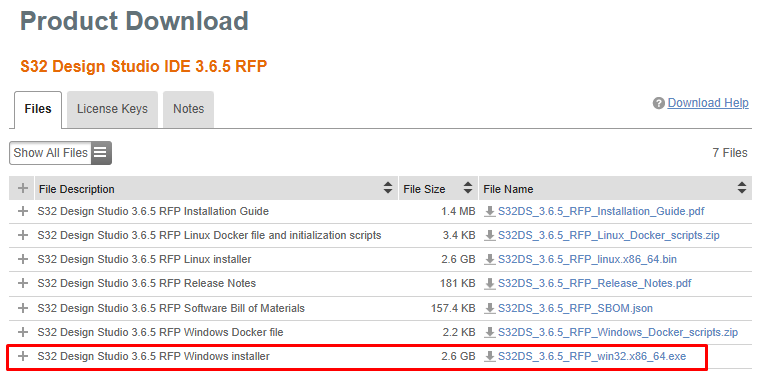
获取软件
-
配置硬件
-
构建和调试
-
构建、运行
1. 开箱即用
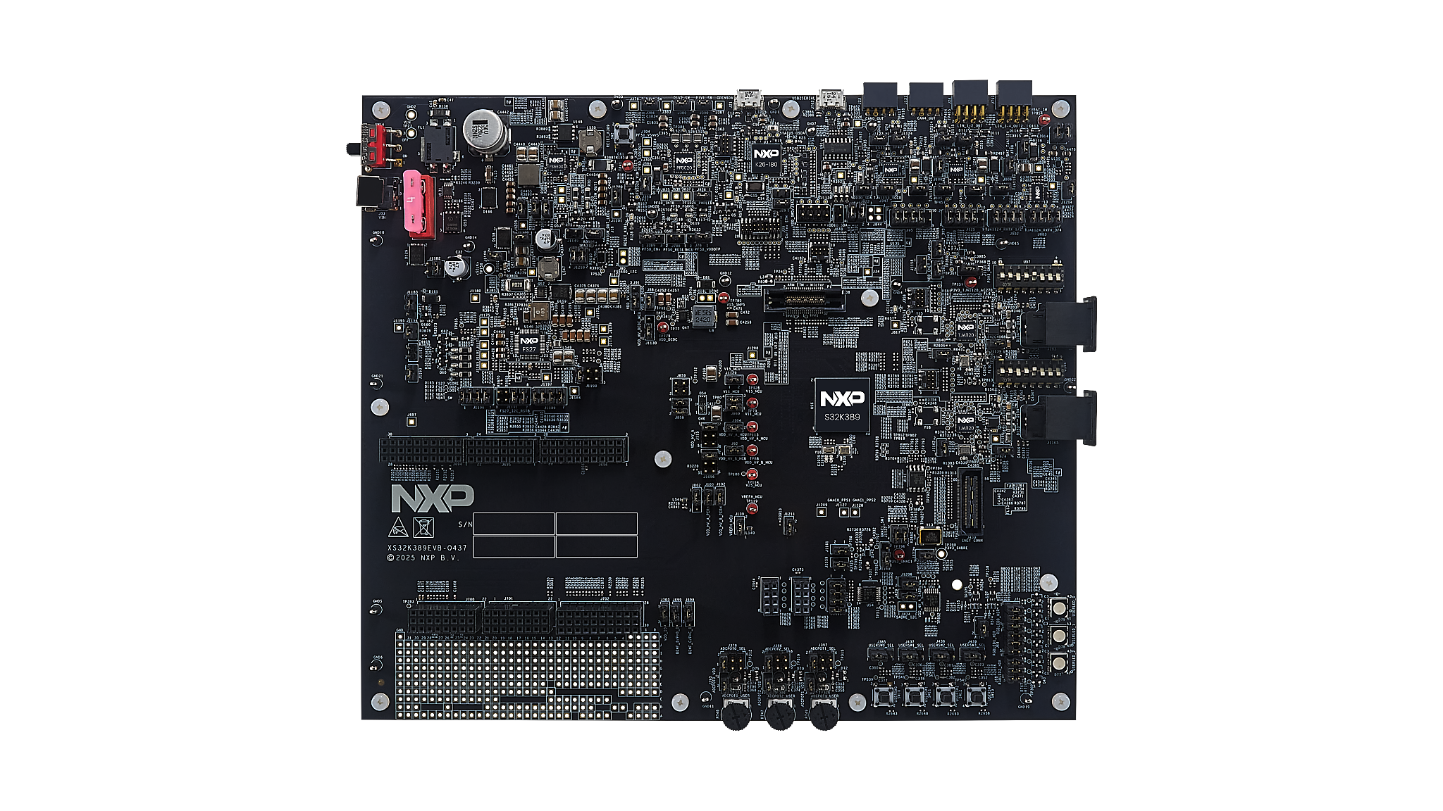
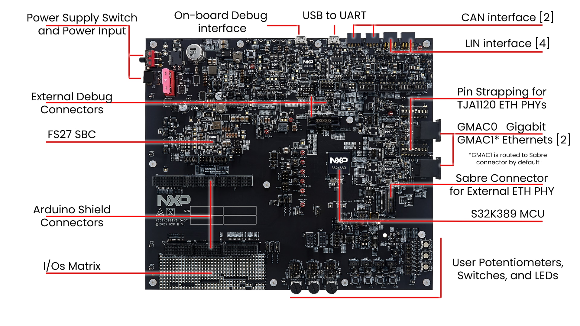
1.1 S32K389EVB-Q437评估板介绍

2. 获取软件
使用您的账号登录恩智浦官网
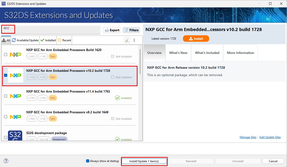
2.2 安装GCC v10.2
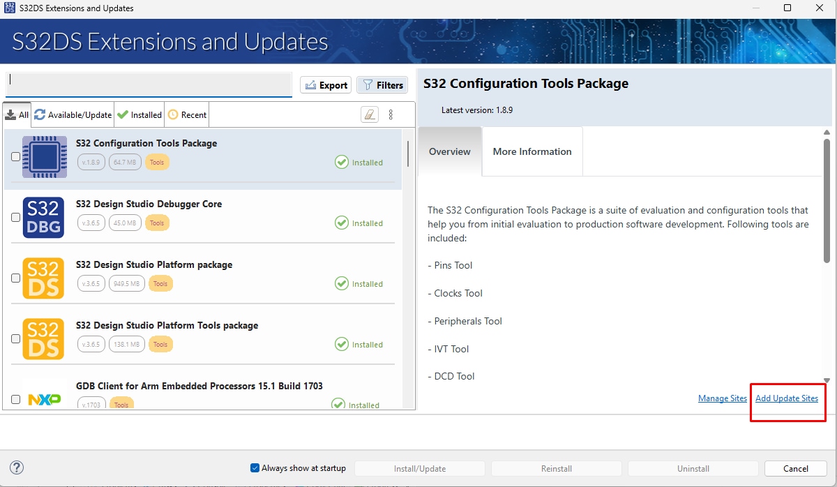
在S32DS中,从顶部菜单转到Help→S32DS Extensions and Updates(帮助→S32DS扩展和更新),打开“S32DS扩展和更新”对话框。
安装GCC v10.2 (当前实时驱动程序所需)
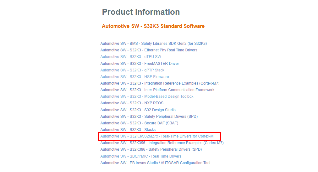
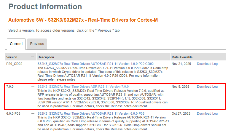
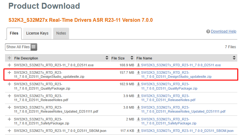
2.4 安装RTD驱动程序
在S32DS中,从顶部菜单转到Help→S32DS Extensions and Updates(帮助→S32DS扩展和更新),打开“S32DS扩展和更新”对话框。点击Add Update Sites(添加更新站点),并浏览下载的RTD *.zip。也可以使用拖放操作将updatesite添加到S32DS。
查找、选择并安装(全部)S32K3实时驱动程序ASR R23-11 V7.0.0。
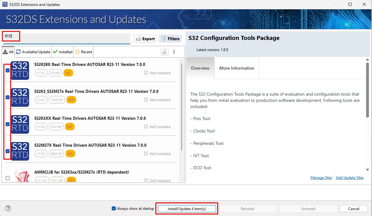
安装完成后,重启S32DS。
2.5 获取FreeMASTER运行时调试工具
S32K389EVB-Q437采用FreeMASTER运行时调试工具进行调试效果更好。
下载并安装FreeMASTER运行时调试工具
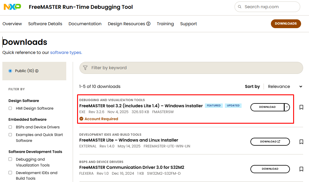
在MCU侧,需要FreeMASTER通信驱动程序
在S32DS中,从顶部菜单转到Help→S32DS Extensions and Updates(帮助→S32DS扩展和更新),打开“S32DS扩展和更新”对话框。
选择并安装FreeMASTER通信驱动程序。
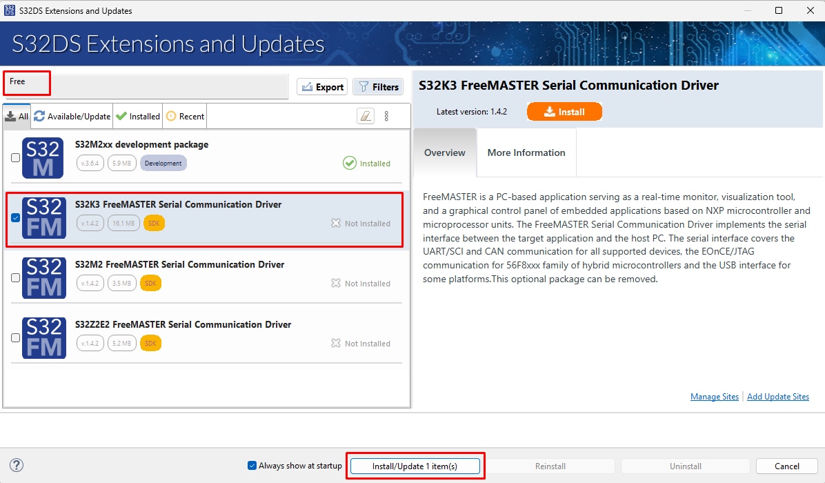
安装FreeMASTER通信驱动程序
安装完成后,重启S32DS。
3. 配置硬件
3.1 将跳线设置到默认状态
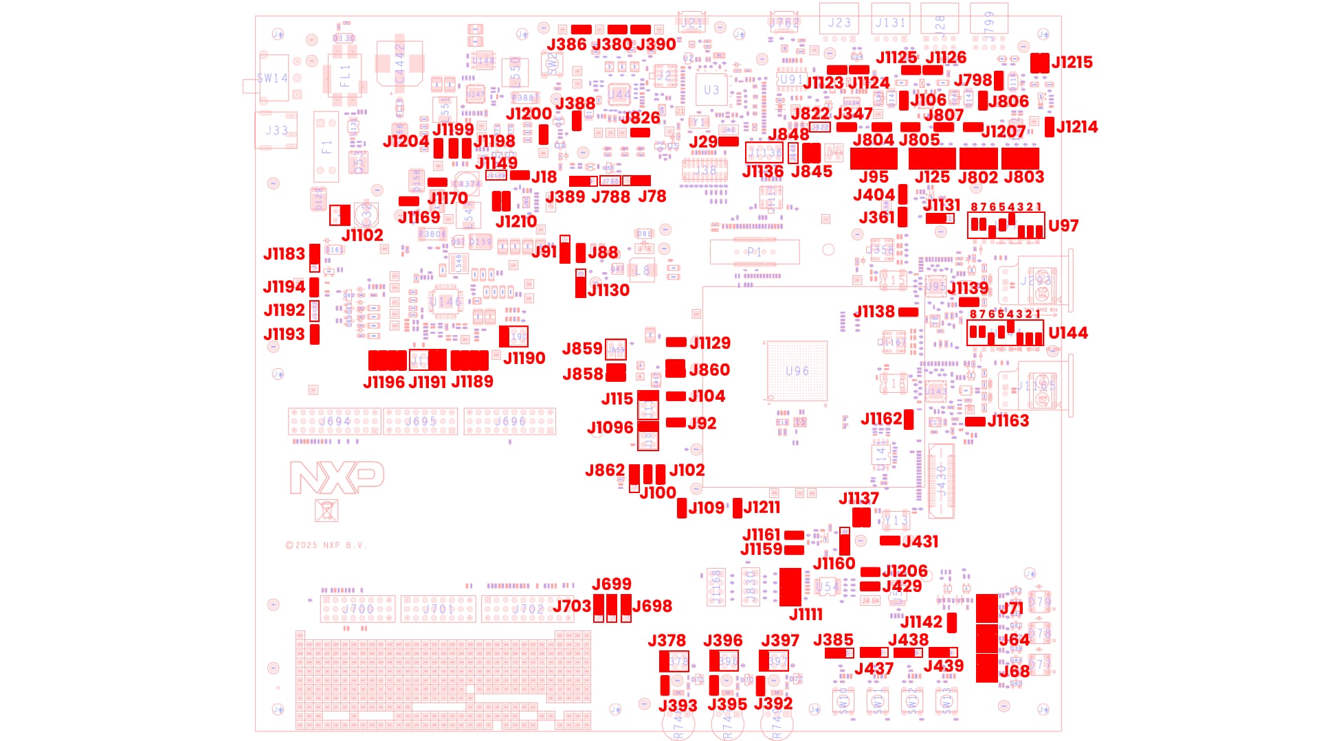
| 跳线 | 状态 | 注释 | |
|---|---|---|---|
| VBAT输入 | J1102 |
1-2 | 过压保护、欠压保护及防反接保护已启用。 |
J1214 |
闭合 | 启用单向电源开关U150的输入。 | |
J1215 |
1-3,2-4 | 分别连接单向电源开关U150的输入与输出。 | |
| FS27/SBC电源 | J1169 |
闭合 | VBAT连接到VBAT_FS27。 |
J1170 |
闭合 | VBAT_FS27连接至FS27接口和VSUP域。 | |
J1183 |
1-2 | FS27调试选项选择。FS27_VDEBUG源自FS27_VBOS。 | |
J1189 |
1-2,3-4,5-6,7-8 | FS27和MCU之间的SPI连接(LPSPI3)。 | |
J1190 |
1-2 | FS27 WAKE1连接至MCU的PTA8(EXTWAKE)。 | |
J1191 |
5-6,7-8 | FS27_RESET和FS27_WAKE2都连接至RESET_MCU。 | |
J1192 |
断开 | FS27_GPIO1信号 | |
J1193 |
闭合 | FS27电压域LED指示灯已启用。 | |
J1194 |
闭合 | FS27 GPIO2连接至MCU的PTA9(PGOOD)。 | |
J1196 |
1-2,3-4,5-6,7-8 | FS27 FS0B和FS1B连接至MCU,FS27_FCCU与FCCU MCU信号之间的FS27 FCCU相连。 | |
| FS5600 | J18 |
闭合 | FS5600电压域LED指示灯已启用。 |
J1149 |
断开 | RESET_MCU与FS5600 PGOOD信号断开连接。 | |
J1198 |
闭合 | FS5600 EN1通过上拉电阻连接至FS27_VPRE。 | |
J1199 |
闭合 | FS5600 EN2通过上拉电阻连接至FS27_VPRE。 | |
J1200 |
闭合 | P3V3SW_OUT1连接至FS5600 SW2开关稳压器——3.3V,10A。 | |
J1204 |
闭合 | P5V0SW_OUT连接至FS5600 SW1开关稳压器——5V,3A。 | |
J1210 |
1-2,3-4 | FS5600 I²C信号连接至MCU。 | |
| PF5020 | J78 |
1-2 | PF5020 OTP编程输入电源电压=GND。 |
J380 |
闭合 | PF50_SW1OUT_1V2跳线使能1.2V输出。 | |
J386 |
闭合 | PF50_SW1OUT_1V8跳线使能1.8V输出。 | |
J388 |
闭合 | P5V0SW_OUT为PF5020 VIN供电。 | |
J389 |
1-2 | PF5020输出通过上拉电阻使能电源。 | |
J390 |
闭合 | PF50_SW1OUT_1V1跳线使能1.1V输出。 | |
J788 |
断开 | PF5020 RESET与RESET_MCU信号断开连接。 | |
J826 |
闭合 | PF5200电压域LED指示灯已启用。 | |
| S32K389 MCU电源 | J88 |
闭合 | 将输入电压连接至MCU的VDD_DCDC。 |
J91 |
1-2 | 选择P3V3SW_OUT1作为MCU的VDD_DCDC的电源。 | |
J92 |
闭合 | 将选定的VDD_HV_B连接至VDD_HV_B_MCU。 | |
J100 |
闭合 | VDD_HV_A_PERH为VDD_HV_A外设提供电压参考。 | |
J102 |
闭合 | VDD_HV_B_PERH为VDD_HV_B外设提供电压参考。 | |
J104 |
闭合 | 将选定的VDD_HV_A连接至VDD_HV_A_MCU。 | |
J109 |
闭合 | 连接VDD_HV_A_MCU和VDD_VREFH_MCU。 | |
J115 |
1-2 | FS27_LDO1_OUT连接至VDD_HV_A. 5V输出 | |
J858 |
1-2,3-4 | FS27_VCORE连接至V15 MCU 1.5V输出。 | |
J859 |
断开 | FS27_VCORE与V15_SMPS开关稳压器断开连接。 | |
J860 |
1-2,3-4 | V11 MCU连接。该跳线使能V11电源与MCU之间的连接。 | |
J862 |
1-2 | 为VDD_REFH_MCU外设提供的电压参考取自VDD_HV_A。 | |
J1096 |
1-2 | FS27_LDO2_OUT连接至VDD_HV_B. 3.3V输出。 | |
J1129 |
闭合 | V15 MCU连接。该跳线使能V15电源与MCU之间的连接。 | |
J1130 |
1-2 | 如果不需要SMPS,则VDD_DCDC必须连接至VDD_HV_B_MCU。 | |
| JTAG | J29 |
闭合 | 从VDD_HV_A_PERH到VDD_SWD/JTAG的电压供应,为JTAG接口供电 |
J1211 |
闭合 | 将RESET_MCU信号连接至MCU PTA5引脚。 | |
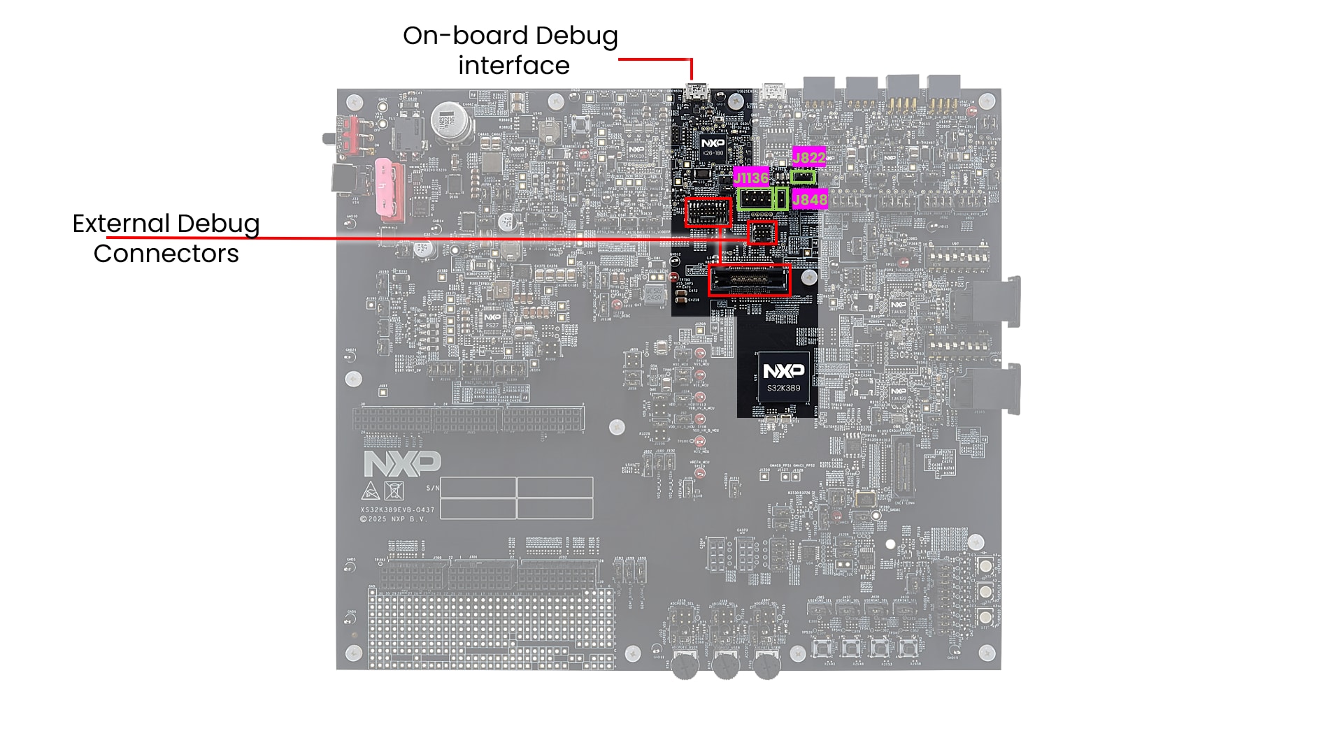
| 板载调试器 | J822 |
断开 | 通过VDD_HV_A_PERH启用VDDIO_SDA的供电。 |
J848 |
断开 | 禁用来自RESET_MCU信号的SDA复位。 | |
J1136 |
断开 | 板载调试器JTAG信号与MCU断开连接。 | |
| SABRE连接器 | J429 |
闭合 | 该跳线使能VDD_HV_A_PERH和VDD_HV_A_SABRE之间的连接。 |
J431 |
闭合 | 启用从P3V3_GMAC1到SABRE连接器的供电。 | |
J1111 |
1-2,3-4,5-6,7-8 | MCU LPSPI4信号连接至SABRE连接器。 | |
J1137 |
1-2,3-4 | GMAC1 MDC功能连接至PTA28,GMAC1 MDIO功能连接至PTA29。 | |
J1206 |
闭合 | MCU LPSPI4 CS1信号连接至SABRE连接器。 | |
| GMAC0 TJA1120_A | J361 |
闭合 | 连接单向电源开关U124的输入。 |
J404 |
闭合 | 启用单向电源开关U124的输入。 | |
J1131 |
1-2 | 旁路单向电源开关U124的输出。 | |
J1138 |
闭合 | 将MCU的PTB4连接至TJA1120_A的中断引脚。 | |
J1139 |
闭合 | 将MCU的PTD13连接至TJA1120_A的唤醒引脚。 | |
J1142 |
闭合 | 将MCU的PTG12连接至TJA1120_A的复位引脚。 | |
| U97-1 | + | GMAC0引脚绑定Config0——上拉。 | |
| U97-2 | + | GMAC0引脚绑定Config1——上拉。 | |
| U97-3 | + | GMAC0引脚绑定Config2——上拉。 | |
| U97-4 | - | GMAC0引脚绑定Config3——下拉。 | |
| U97-5 | 0 | GMAC0引脚绑定Config4——断开。 | |
| U97-6 | + | GMAC0引脚绑定Config5——上拉。 | |
| U97-7 | 0 | GMAC0引脚绑定Config6——断开。 | |
| U97-8 | 0 | GMAC0引脚绑定TJA1120_RST——断开。 | |
| GMAC1 TJA1120_B | J1159 |
闭合 | 连接单向电源开关U142的输入。 |
J1160 |
1-2 | 旁路单向电源开关U142的输出。 | |
J1161 |
闭合 | 启用单向电源开关U142的输入。 | |
J1162 |
闭合 | 将MCU的PTB26连接至TJA1120_B的中断引脚。 | |
J1163 |
闭合 | 将MCU的PTA31连接至TJA1120_B的唤醒引脚。 | |
| U144-1 | + | GMAC1引脚绑定Config0——上拉。 | |
| U144-2 | + | GMAC1引脚绑定Config1——上拉。 | |
| U144-3 | + | GMAC1引脚绑定Config2——上拉。 | |
| U144-4 | - | GMAC1引脚绑定Config3——下拉。 | |
| U144-5 | 0 | GMAC1引脚绑定Config4——断开。 | |
| U144-6 | + | GMAC1引脚绑定Config5——上拉。 | |
| U144-7 | 0 | GMAC1引脚绑定Config6——断开。 | |
| U144-8 | 0 | GMAC1引脚绑定TJA1120_RST——断开。 | |
| CAN0接口 | J95 |
1-2,3-4,5-6,7-8,9-10 | 将MCU的CAN0控制引脚连接至CAN PHY U134 TJA1463。 |
J106 |
闭合 | 启用从VBAT到CAN0收发器的电源。 | |
J347 |
闭合 | 启用从P5V0SW_OUT到VCC收发器引脚的5V电源。 | |
J804 |
闭合 | 为VIO引脚选择供电电压——VDD_HV_A_PERH。 | |
J1123 |
闭合 | 将CAN0_H连接至60Ω终端电阻。 | |
J1124 |
闭合 | 将CAN0_L连接至60Ω终端电阻。 | |
| CAN4接口 | J125 |
1-2,3-4,5-6,7-8,9-10 | 将MCU的CAN4控制引脚连接至CAN PHY U135 TJA1443。 |
J805 |
闭合 | 启用从P5V0SW_OUT到VCC收发器引脚的5V电源。 | |
J806 |
闭合 | 启用从VBAT到CAN0收发器的电源。 | |
J807 |
闭合 | 为VIO引脚选择供电电压——VDD_HV_B_PERH。 | |
J1125 |
闭合 | 将CAN4_H连接至60Ω终端电阻。 | |
J1126 |
闭合 | 将CAN4_L连接至60Ω终端电阻。 | |
| LIN接口 | J798 |
闭合 | 将VBAT连接至LIN PHY U87 TJA1124。 |
J802 |
1-2,3-4,5-6,7-8 | 将LPUART9_TX/RX和LPUART12_TX/RX连接至LIN PHY U87 TJA1124的LIN1和LIN2。 | |
J803 |
1-2,3-4,5-6,7-8 | 将LPUART13_TX/RX和LPUART8_TX/RX连接至LIN PHY U87 TJA1124的LIN1和LIN2。 | |
J1207 |
闭合 | 将VDD_HV_A_PERH连接至LIN PHY U87 TJA1124的VIO。 | |
| USB转串口桥 | J845 |
1-2,3-4 | 将LPUART11_TX/RX连接至USB2UART转换器U91 MCP2221。 |
| 用户外设 | J64 |
1-2,3-4,5-6 | 将MCU的通用IO连接至RGB LED D78控制引脚。 |
J68 |
1-2,3-4,5-6 | 将MCU的通用IO连接至RGB LED D77控制引脚。 | |
J71 |
1-2,3-4,5-6 | 将MCU的通用IO连接至RGB LED D79控制引脚。 | |
J378 |
1-2 | 将MCU的PTA11连接至ADCPOT0_USER电阻。 | |
J385 |
1-2 | 将MCU的PTA1连接至用户开关0。 | |
J392 |
闭合 | 将VDD_REFH_PERH连接至ADCPOT1_USER电阻。 | |
J393 |
闭合 | 将VDD_REFH_PERH连接至ADCPOT0_USER电阻。 | |
J395 |
闭合 | 将VDD_REFH_PERH连接至ADCPOT2_USER电阻。 | |
J396 |
1-2 | 将MCU的PTA18连接至ADCPOT2_USER电阻。 | |
J397 |
1-2 | 将MCU的PTA17连接至ADCPOT1_USER电阻。 | |
J437 |
1-2 | 将MCU的PTB8连接至用户开关1。 | |
J438 |
1-2 | 将MCU的PTA23连接至用户开关2。 | |
J439 |
1-2 | 将MCU的PTE11连接至用户开关3。 | |
| ARDUINO连接器 | J698 |
1-2 | BEMF_C/PHC_I信号连接至PTE0引脚。 |
J699 |
1-2 | BEMF_B/PHB_I信号连接至PTE1引脚。 | |
J703 |
1-2 | VDD_IO引脚连接至VDD_HV_A_PERH。 |
3.2 给板上电
将SW14切换到OFF位置(完全向上)。
连接12V电源适配器,将SW14开关置于ON位置(完全向下)。
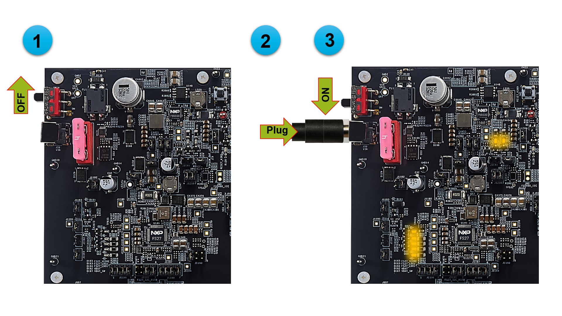
当EVB上电时,稳压器旁边的橙色LED显示存在电源电压。
4. 构建和调试
立即试用S32K389EVB-Q437评估板。
4.1 从头开始创建新的S32DS项目
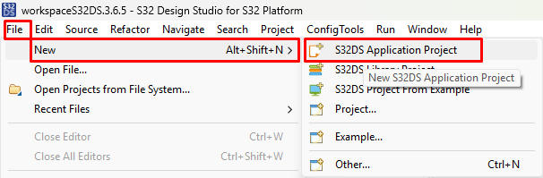
启动S32 Design Studio 3.6.5。转到menu → File → New → S32DS Application Project(菜单→文件→新建→S32DS应用项目)
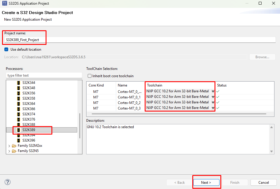
填写新项目名称(无空格),选择S32K389衍生产品。
选择GCC版本10.2,而不是默认版本11.4。已安装的S32K3 RTD V7.0是为GCC toolchain 10.2创建的。
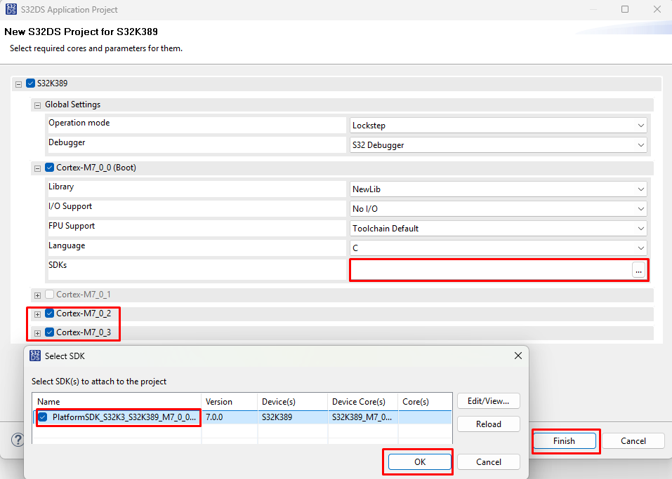
为主核Core 0选择SDK (S32K3 RTD V7.0)。Core 1是锁步配置中Core 0的检查器内核。也可以为Core 2和3选择SKD。
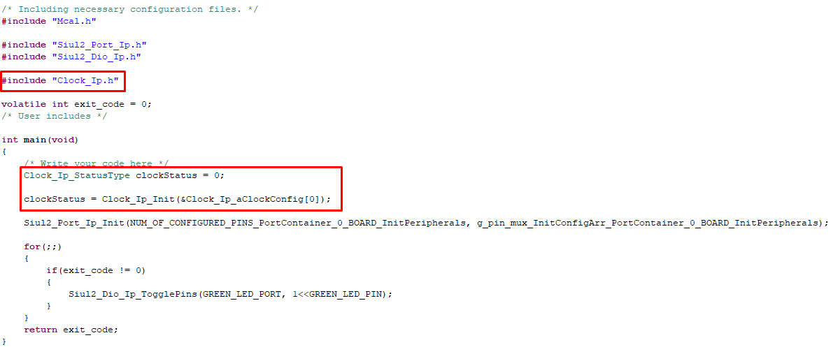
4.2 设置引脚
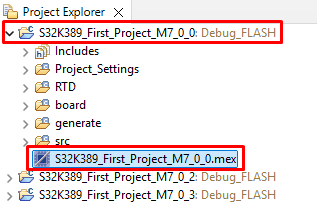
1. 双击项目mex文件
2. 将PTI30引脚(连接至绿色LED)设置为GPIO输出
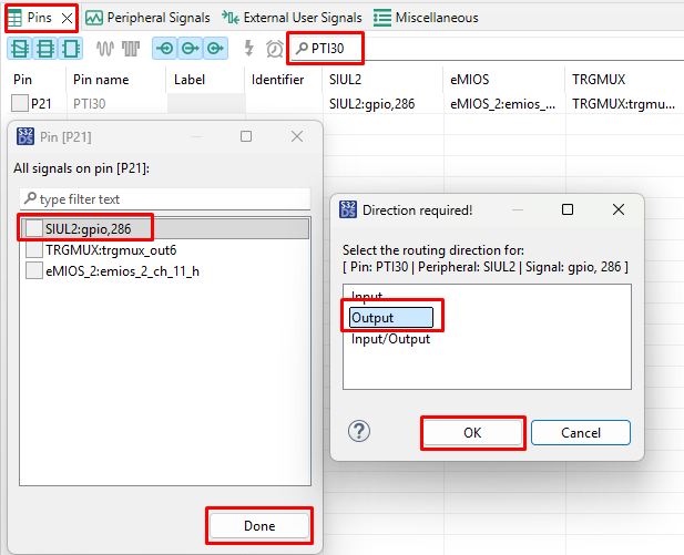
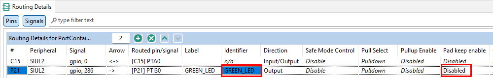
3. 定义PTI30标识符(无空格)。例如"GREEN_LED"。对“管脚保持启用”选项选择“禁用”。
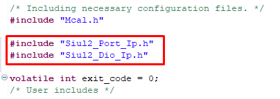
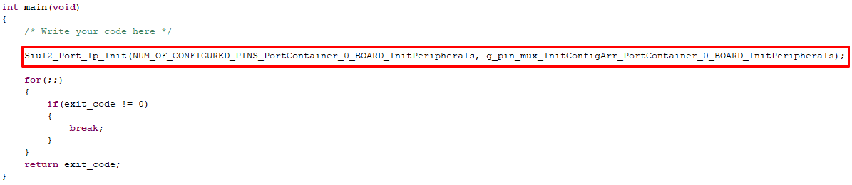
4.3 添加驱动程序,生成配置文件
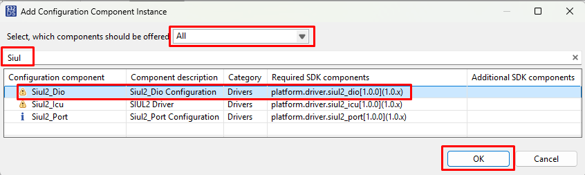
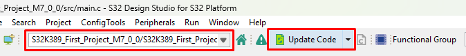
切换到外设视图,将Siul2_Dio驱动程序添加到应用中。

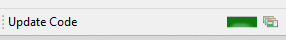
请确定配置了适当的项目,然后点击"Update Code"(“更新代码”)按钮生成配置文件。
等待更新代码结束。状态栏位于右下角。

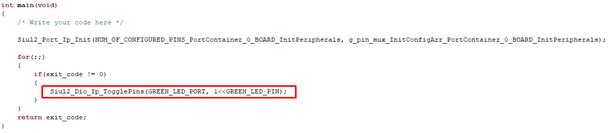
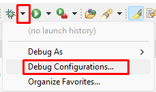
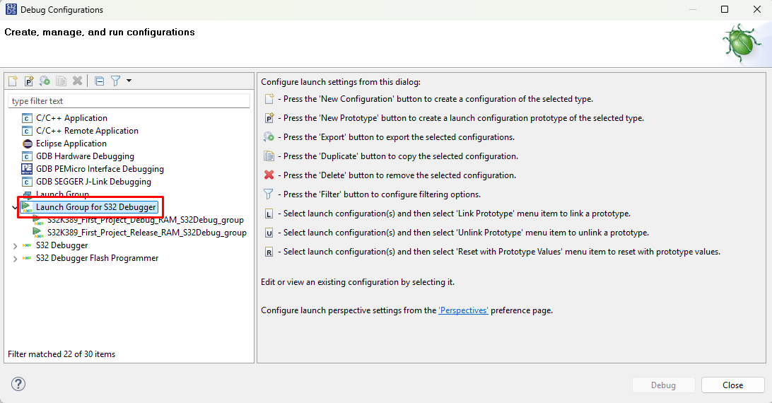
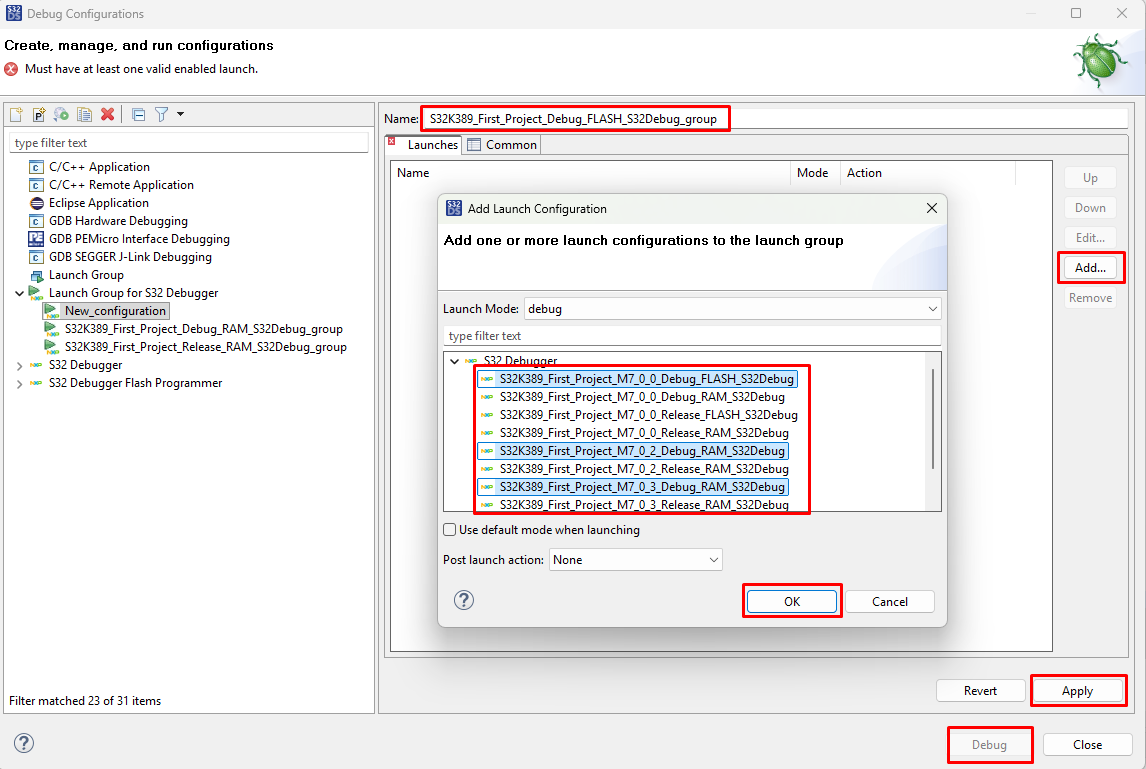
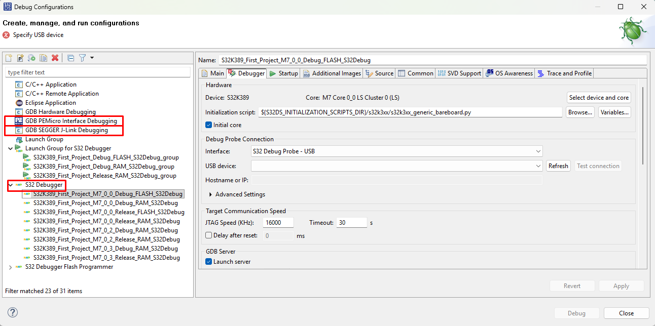
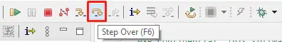
5. 构建、运行
5.1 将软件上传到MCU
使用Debug Configuration (调试配置)菜单,选择“启动组”配置,为所有内核构建和上传软件项目。