One number sits underneath every semiconductor test program, and it rarely gets the attention it deserves—fault
coverage. Fault coverage is the percentage of possible defects in a chip that the test program can detect with
everything else in the test economics connecting back to it.
Understanding fault coverage, the cost pressure that surrounds it and the design-stage decisions that determine its
ceiling is what separates a test strategy from a test habit.
What Fault Coverage Actually Measures
Fault coverage is not a measure of how thoroughly a chip has been tested in any intuitive sense. It measures how many
possible failure modes are visible to the test. A fault coverage of 95% does not mean that the chip is 95% tested.
Rather, it means that as they are invisible, 5% of possible failure modes will not be caught on the production floor
and might be found by the end user.
That distinction matters because coverage is not free at the margin. The last few percentage points target the
failure modes that are hardest to reach, and they are the most expensive to achieve. They require more test time,
more sophisticated test content and depend on how the chip was designed to be tested in the first place. This is
where the economics of fault coverage intersect with those of the test floor.
The Cost of a Millisecond
High-volume semiconductor production runs at a scale where small per-chip variables become large total costs. A test
program that takes one second longer per chip—across a production run of tens of millions of units—can add up to
hundreds of hours of additional tester time. Test time is one of the most actively managed variables on the
production floor because of the cost structure behind the equipment that runs the test.
An automatic test equipment (ATE) system is a capital asset that often runs into millions of dollars per unit. Its
cost is amortized across the test hours that it delivers over its working life, and that depreciated hourly rate
factors directly into the cost per good unit shipped. The test contribution to cost of goods is determined by
multiplying the test time per chip by the loaded hourly rate and dividing by the yield.
The main lever for managing this is multisite testing, where several chips are tested in parallel on the same ATE.
Higher site counts mean that a single tester produces many tested devices per second rather than one. Doubling the
site count does not exactly halve the effective test time per chip because some overhead does not scale with
parallelism, but it comes close. Beyond multisite, test programs are tuned continuously—instrument settings
optimized for speed, and content that does not contribute to coverage removed.
Cost Versus Coverage
To further illustrate the scale of test-time economics, take for example a loaded tester rate of $0.10 per second and
a chip that needs two seconds of test time. Tested one at a time that is $0.20 of test cost per chip but testing two
in parallel roughly half the effective test time per chip dropping the cost to around $0.10. That difference seems
trivial until you consider the volume. Across twenty million units, a $0.10 saving per chip is two million dollars,
depending almost entirely on how many chips the tester handles at once.
Removing test content is when the trade-off occurs. If test time needs to be driven down, and test content is a
factor in how long a test takes, the next question is what happens when the cost pressure runs into the requirement
to maintain coverage.
The Tension and Why Resolving It Requires More Than Engineering
Test time and fault coverage pull in opposite directions. The cost pressure (as outlined in the previous section) is
straightforward: reducing test time to lower the cost per good unit. Reducing test time without reducing test
content means to achieve the same coverage faster, which is possible but has limits. Reducing test time by removing
test content means that while coverage falls—as indicated by the non-linear relationship referenced above—even a
modest fall in coverage can produce a meaningful increase in escapes.
This is not a problem that engineering can resolve on its own, because the answer depends on a business context
separate from the engineering process considering factors such as:
- How many escapes are acceptable?
- At what field return cost?
- For which customers?
A consumer electronics manufacturer and an automotive supplier looking at the same coverage number are looking at
fundamentally different risk profiles.
Acceptable defect levels in consumer electronics are typically measured in defective parts per million (DPPM.) In
automotive and industrial segments, the relevant unit is defective parts per billion (DPPB), tightening the bar a
thousand-fold. The difference is not simply a matter of customer preference. Rather, it reflects the regulatory and
liability exposure that comes with a field failure in a safety-critical system, which is fundamentally different
from the exposure of failure in a consumer device.
Setting fault coverage is therefore a business decision with quantifiable financial consequences on both sides of the
equation. It sits at the intersection of cost and quality, and it benefits from being treated as such rather than as
a question for either side alone.
DFT is the Lever that Sets the Ceiling
Fault coverage and test time are both managed on the production floor once the chip physically exists, but there is
also a powerful lever at play earlier in the process.
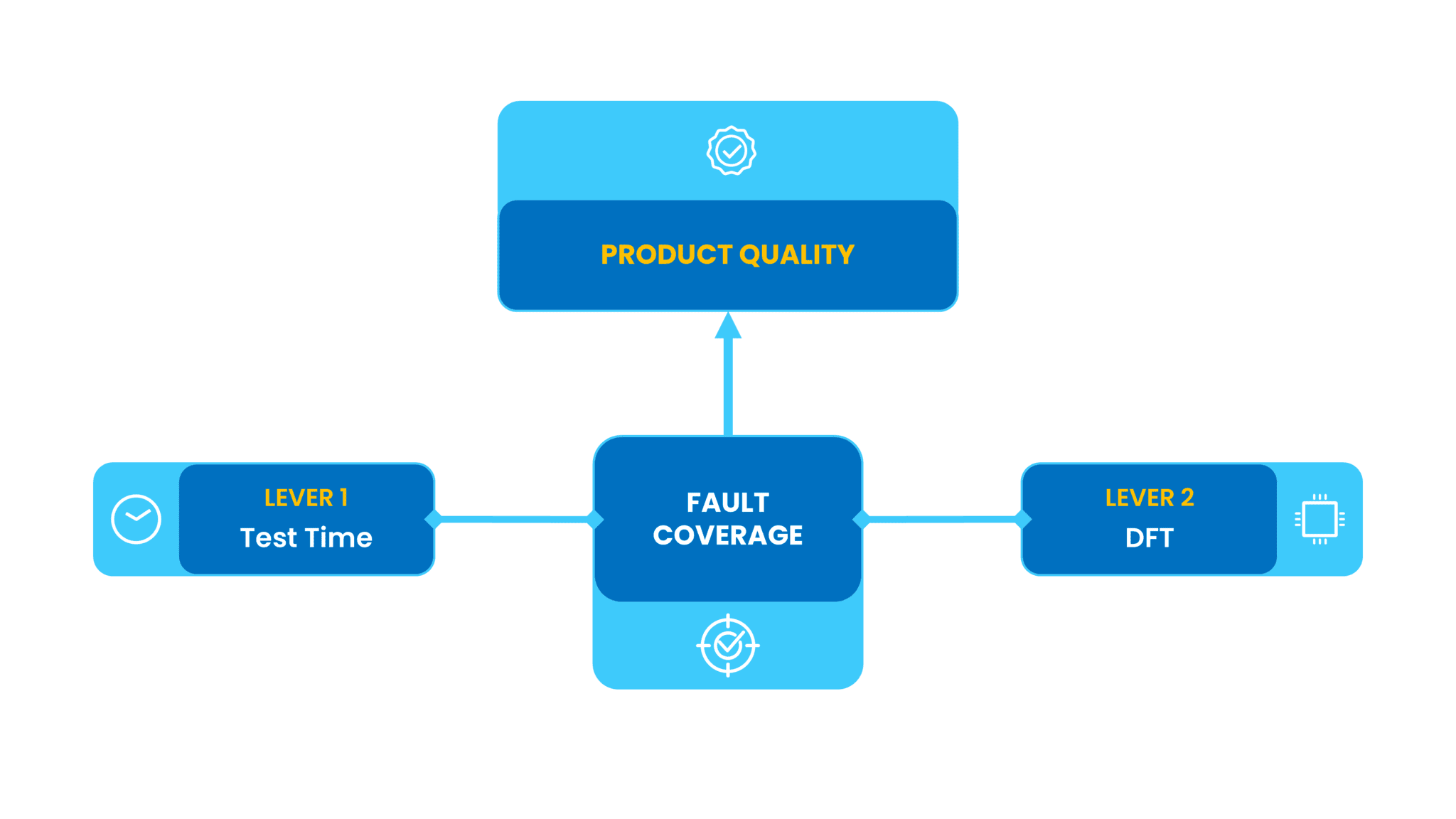
Fault coverage is influenced by two management levers: test efficiency during
production and testability during design.
Design for testability (DFT) refers to building test access into the chip at the design stage, before manufacturing
begins. One concrete example is the built-in self-test (BIST) logic embedded inside the chip that allows it to test
parts of its own functionality without relying entirely on external ATE. A chip with well-designed BIST can achieve
higher fault coverage in less time because some of the test infrastructure is already inside the device rather than
being applied from outside.
DFT is broader than BIST in that it covers the design-stage decisions that determine how accessible the chip's
internal state is to a test program. One common example is scan chains that link the chip's internal elements into a
structured path, allowing the tester to load specific states into the chip through this path and read the results
the same way. This makes parts of the chip visible that would otherwise be hidden. A chip designed with testability
in mind gives the test engineer something to work with. A chip designed without it puts a cap on achievable coverage
that cannot be raised after the fact.
Because DFT comes at a cost, it impacts the economic character. It consumes silicon area—with the exact share
depending on the design and the methodology chosen—and it adds on engineering time before the design is finalized.
Design and test teams weigh these trade-offs together—area and schedule on one side, coverage and product quality on
the other. It is a joint decision based on the same goal product that meets its quality requirements at a cost that
supports the business.
Why DFT Decisions Matter Before Tape-Out
Investing in DFT before tape-out buys coverage at the cheapest point in the flow. Compensating for limited DFT on the
test floor through separate test steps in the production flow such as longer test times or additional test
insertions, raises the cost on every chip produced. Absorbing the consequences of insufficient coverage in the field
is the most expensive option of all, defects missed during production return in the form of recalls or liability.
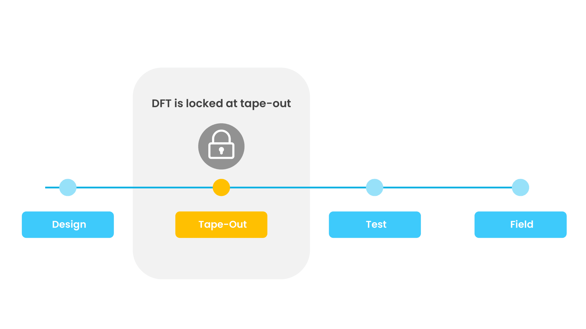
What makes DFT different from other test investments is irreversibility. Test step durations, test limits and
multisite configurations can all be adjusted later, but DFT decisions are locked in at design time. Once a chip has
been taped out and the finalized design is sent to the foundry, the testability of that chip is fixed. If a
product's DFT does not support the fault coverage needed to meet its quality requirements, no remediation can be
given on the test floor, and the gap cannot be closed.
Unlike test programs and production settings, DFT decisions become largely
irreversible once a design is taped out.
The Decision That Shapes Everything Going Forward
Every other lever in test engineering operates after the chip has already been manufactured. Test time can be
compressed; test limits can be tightened or loosened, and multisite configurations can add throughput. All those
levers are adjustable, yet all of them are constrained by what the chip's design allows.
DFT is the one decision in the test flow that cannot be revisited later. It is made early, before production data
exists to validate it, and against competing demands on silicon area and design schedule. The further decision sits
from a clear view of the product's end-market quality requirements, the harder it is to calibrate well. Bringing
that market view earlier in the design phase—rather than during the test floor phase—is what turns DFT from a
technical choice into a strategic one.
In an industry where a single significant escape event can carry hundreds of millions of dollars in recalls and
liability costs, deciding what testability to build into a chip before it is manufactured not an engineering detail.
Rather, it is a strategic commitment—one that defines the options available at every stage that follows.