Every test step in a semiconductor manufacturing flow represents a decision: the value that it adds must justify the
cost it adds. Sometimes that decision is explicit, written into a business case. Just as often, it is engineered
into the flow as an established practice, grounded in years of accumulated data on where defects appear and what it
costs to detect them, but the underlying judgment is the same: finding a failure at this point in the flow is worth
the cost. That is not a quality statement, rather it is a financial one.
Three ideas sit behind that judgment. First, a test does not produce perfect results, rather it acts as a filter. And
like any real-world filter, its selectivity is finite. Second, the cost of a defect depends heavily on where it is
found in the flow with that cost rises sharply at every downstream step. Third, some defects remain invisible
through every chip test, potentially surfacing later once the device is already in service.
How a Test Works and Why No Filter is Perfect
A test does not directly sort chips into good and bad quality. It sorts them into passes and fails based on whether
each device meets a defined set of electrical criteria. Those two categories usually overlap with whether a chip is
functional or defective, but not always. The test is a filter, and like any filter applied to a population that
varies in subtle ways, its selectivity is finite with some chips ending up on the wrong side of the line.
A chip that fails the test but is functional is called a false reject. Each false reject is still a functional chip
that has been screened out and scrapped. The cost is immediate and direct: it appears in yield figures, cost per
good unit and the economics of every wafer that runs through the line.
A chip that passes the test but is defective is called an escape. If that chip ships, gets embedded in a product and
fails later, the cost does not surface on the test floor. It surfaces at the customer, at incoming inspection, in
the field during use or, in the most demanding applications—somewhere with consequences well beyond a warranty
claim.
These two outcomes pull against each other. Tighten test limits, and the number of escapes goes down while the yield
loss rises. Loosen them, and yield recovers while defective devices are more likely to reach end users. The position
a company chooses on that spectrum reflects a deliberate judgment about which cost is more acceptable depending on
the product, the customer base and the consequences of each type of error in the specific market being served.
Escapes are unavoidable in any real-world filter. The discipline is in to manage where the trade-off lies, and in
doing so with a clear view of the cost of each side of that trade-off.
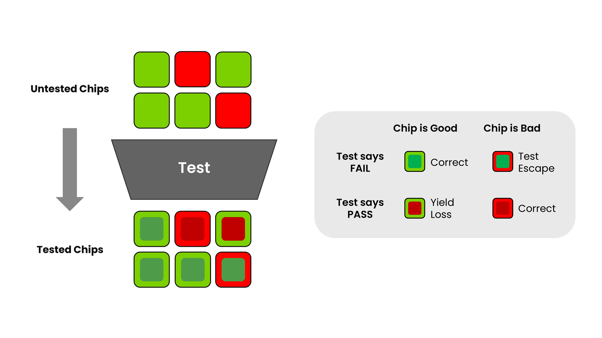 Semiconductor tests act as filters. Good chips may be rejected (yield loss), while
defective chips may occasionally escape detection and reach customers.
Semiconductor tests act as filters. Good chips may be rejected (yield loss), while
defective chips may occasionally escape detection and reach customers.
Bright minds. Bright futures. NXP team members create breakthrough technologies that advance our
world. Explore current career opportunities with NXP.
The Rule of Ten: A Pattern That Holds Across Industries
The idea that the cost of a problem depends on where it is detected is not unique to semiconductors. It shows up in
manufacturing, construction, software development and financial services. The most widely used formulation is the
rule of ten, sometimes called the 1-10-100 rule.
- Preventing a defect is the cheapest option
- Once a defect occurs, catching and correcting it internally before it reaches a customer costs roughly 10 times
as much
- Once that failure reaches a customer, costs can rise to roughly 100 times as much
The Rule of Ten Explained
The multipliers are approximate. What matters is the structural pattern they describe. Prevention acts early, before
significant cost has been added to the product. Internal correction acts on a product that already carries an
accumulated investment. External failure acts on a product that has already reached a customer, often embedded in a
larger system, with warranty obligations attached and—depending on the application— the additional regulatory
exposure.
In semiconductor manufacturing, the test flow follows this logic step by step. The same defect carries a different
cost depending on where it is found:
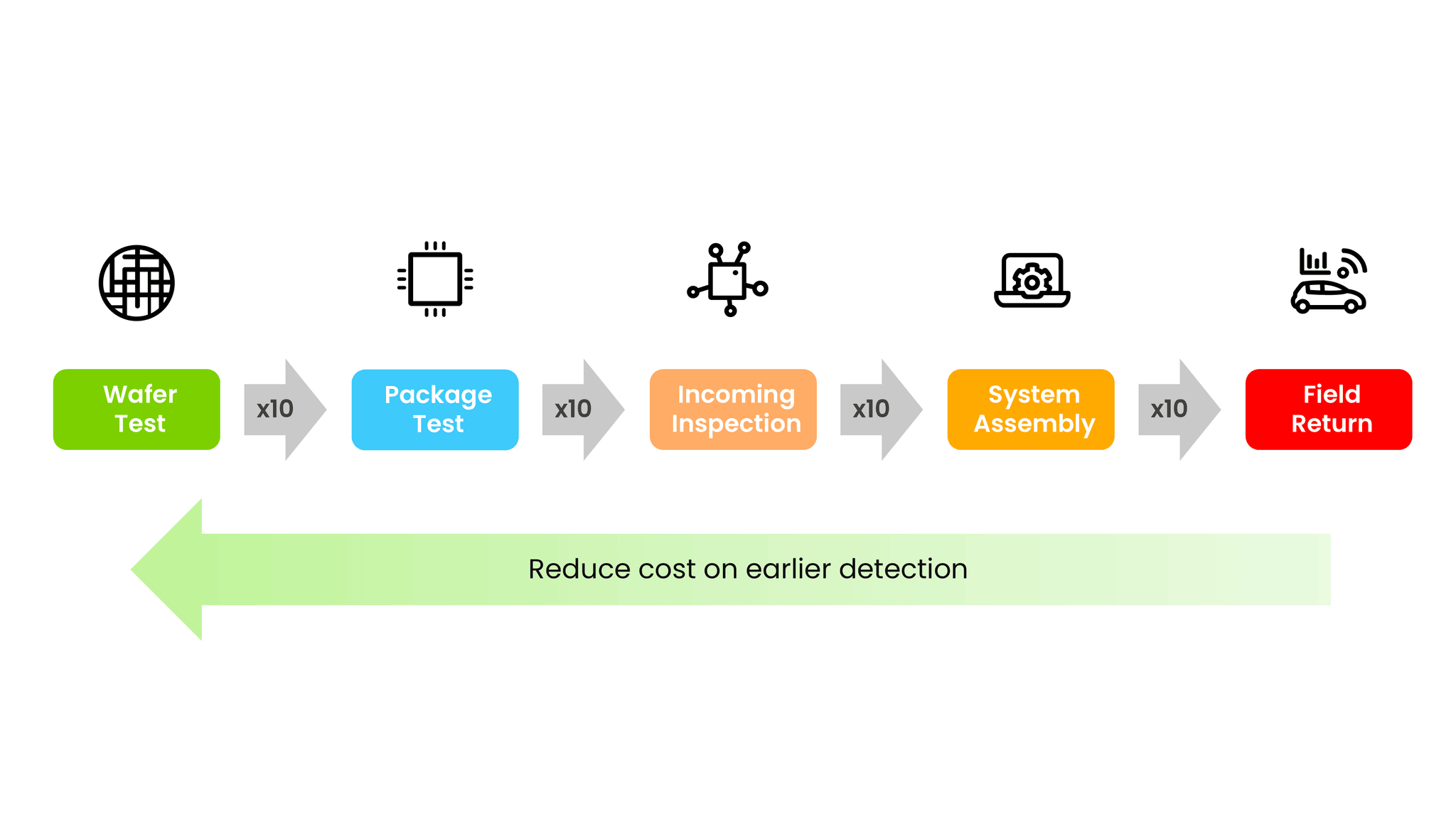 The cost of a defect rises dramatically as detection moves downstream through the
value chain.
The cost of a defect rises dramatically as detection moves downstream through the
value chain.
- Wafer test: The die is marked as failed and excluded before packaging cost is added with a cost of roughly one
- Package test: Packaging has already been applied and the product is worth considerably more than it was on the
wafer with a cost of roughly 10
- Customer incoming inspection: The chip has been shipped, handled and is now in someone else's hands with a
defective cost of roughly 100
- System assembly: The chip is part of a larger product, and removing or replacing it carries the cost of that
whole product, not just the chip with a cost of roughly 1,000
- Field failure: The product is in service meaning returns, logistics, failure analysis, replacements and the
downstream effects on reputation and the customer relationship all stack on top of each other with a cost of
10,000 or more
To put this all in perspective, take for example a defect that would have cost a few cents to screen out during a
wafer test:
- If it is discovered during package test, it only costs the price of the packaged part
- If it is discovered during system assembly, it can cost the price of the entire system the chip went into
- If it is discovered in the field, it triggers a return process with the total cost depending on how the product
is used and where it is used—the jumps compound
- A defect that travels from wafer test to the field has not become 10 times more expensive, rather it has become
ten thousand times more expensive, or more
This is where the asymmetry between false rejects and escapes becomes concrete. A false reject costs the margin on
one chip. An escape that reaches a customer can cost orders of magnitude more, and the further it travels downstream
before being found, the larger that gap grows.
Applying the Rule of Ten
This becomes more than a conceptual framework when numbers are applied. The cost of a test step is known. The escape
rate without that step can be estimated. The average cost of a field return can be measured. When those figures are
assembled, the rule of ten often reveals that the test investment is not just defensible—it is the economically
rational choice, often by a considerable margin.
The calculation shifts when the customer base is segmented. For example, a field return in consumer electronics
carries one cost profile. Meanwhile, a field return in automotive or medical carries another because of the
regulatory. Safety and liability exposure are of a different order entirely. A company that sells predominantly
safety-critical applications operates at a fundamentally different point on the cost curve, and its test investment
decisions should reflect that.
Killer Defects, Latent Defects and the Reliability Layer
The escape rate captures only part of the picture. Not every defect causes a chip to fail at test—some defects cause
immediate detectable failure: killer defects. They show up as yield loss, are counted and are excluded from
shipping.
A second category is smaller, elusive and often more consequential. Latent defects—also called reliability
defects—pass every test that the chip moves through. They ship, enter service and fail later. Sometimes the trigger
is the combination of thermal and electrical stress that the chip encounters in real-world operation. Sometimes it
is extended use reveals a marginal weakness the test was not designed to detect.
Research conducted across multiple device manufacturers has established a consistent statistical relationship between
the two categories. For every 100 killer defects that cause yield loss at test, there are approximately one to two
latent defects that will result in a field reliability failure.¹ The defect types that drive yield loss and those
that drive latent failures are largely the same or are distinguished primarily by their size and by where they
happen to land on the die structure.
What Latent Defects Change
Because latent defects can pass initial testing and fail later in use, manufacturers rely on yield patterns and
stress screening to reduce field-return risk.
First, a high-yield wafer is not necessarily a high-reliability wafer, but a low-yield wafer is statistically more
likely to produce chips with elevated latent defect risk. The lots that perform worst at the test also tend to
generate the most field failures. This is why some manufacturers exclude a chip that passed the test if it sits in a
cluster of failed chips on the wafer. The spatial correlation between yield defects and latent defects can be strong
enough that a passing chip surrounded by failures carries elevated risk, even if it cleared every electrical test.
Second, any escape calculation may undervalue field-return costs when latent defects are involved. The cost ladders
outlined in the previous section—assumes the defect is found at a specific step. Latent defects break that
assumption. They may surface only after the chip has been in service for weeks, months or years, by which time this
failure reaches the deepest and most expensive end of the ladder. The cost is not only the replacement of the chip,
but also the diagnosis, field intervention and—in regulated applications—the ensuing investigation and reporting.
The industry treats this seriously, which is reflected by the test flow. Burn-in exposes chips to elevated
temperature and voltage to accelerate early-life failures, so that latent defects surface in the factory rather than
at the customer. Complementary techniques add further layers. Quiescent supply current (IDDQ) measures quiescent
current to catch subtle electrical anomalies that functional tests can miss, and stress screens chips through
controlled extremes to flush out marginal devices before they ship.
Defect rates are typically measured in parts per million and—in segments with higher quality standards such as
automotive—in parts per billion. These targets drive continuous investment in screening methods, monitoring and
process control. Reliability is treated as something to be actively driven down, not as a residual risk to be
tolerated.
Three Takeaways for Test Economics
In practice, these test economics point to three practical conclusions for how companies balance yield, cost and
downstream risk.
First, test yield is a financial metric with multiple faces. It reflects how efficient upstream processes are, how
much margin is being absorbed by the test limits in use and how much risk is being carried toward customers.
Optimizing one face without minding the others produces decisions that look strong on one metric but are damaging to
another.
Second, the customer segment matters as much as the escape rate itself. Break-even analysis tells a company where a
test investment starts to pay for itself, however it does not tell the company where to stop. In segments where
field returns carry full liability and regulatory exposure, the right level of test investment sits well above that
point. Average costs can hide the tail risk, and in this industry such tail can be very expensive.
Third, catching a defect early is not only about avoiding cost. It is also about where that cost lands in the
organization and how much control the organization keeps over the outcome. It is also about where the organization
the cost lands and how much control the organization keeps over the outcome. A defect caught at wafer test is a
manufacturing issue with a straightforward path to resolution. The same defect found by a customer is a different
kind of problem, involving more functions, more time and considerably less predictability. The earlier the
detection, the more options remain open, and the cheaper those options tend to be as the ability to influence the
outcome shrinks at every step downstream.
That logic holds across industries. In semiconductors, the stakes attached to it are unusually high.
¹Source – Price, D. W., and Sutherland, D. G., Process
Watch: The Most Expensive Defect — Part 2. Semiconductor Digest , 2015.