开始使用S32K388EVB-Q289进行开发
上次修改时间:
2024-10-29 11:45:00支持
S32K388EVB-Q289汽车通用评估板
1. 开箱即用
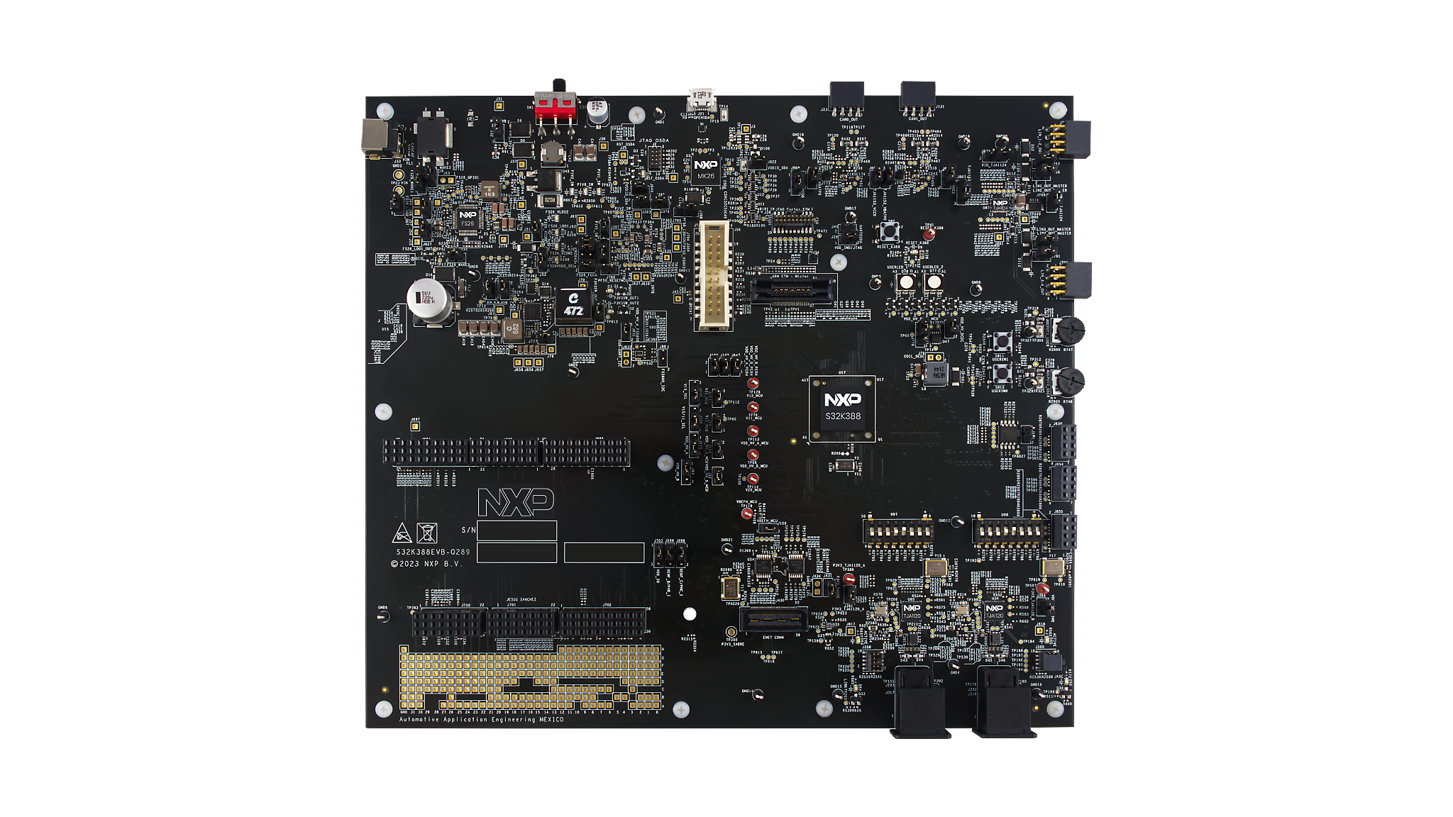
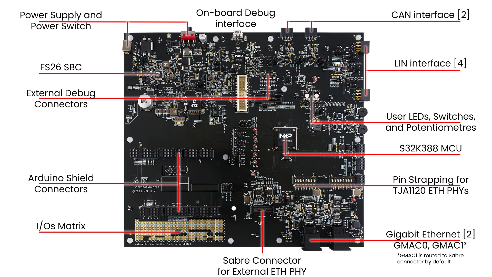
1.1 S32K388EVB-Q289评估板介绍

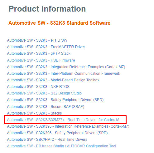
2. 获取软件
您可以观看视频或遵循以下分步指南,安装软件并设置S32K3X8EVB-Q289板:
首先,使用您的账号登录恩智浦官网。
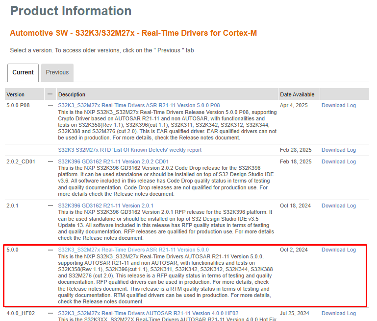
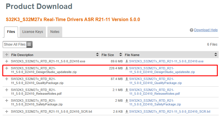
2.3 安装RTD驱动程序
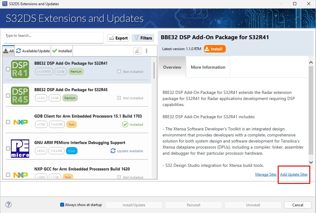
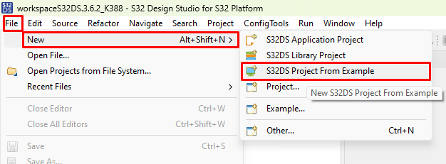
在S32DS中,从顶部菜单转到Help→S32DS Extensions and Updates(帮助→S32DS扩展和更新),打开“S32DS扩展和更新”对话框。点击"Add Update Sites"(添加更新站点),并浏览下载的RTD *.zip。
查找、选择并安装(全部) S32K3实时驱动程序ASR R21-11 V5.0.0。
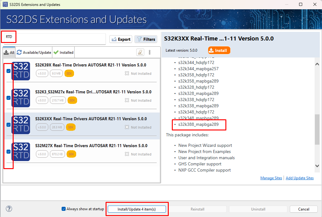
安装完成后,重启S32DS。
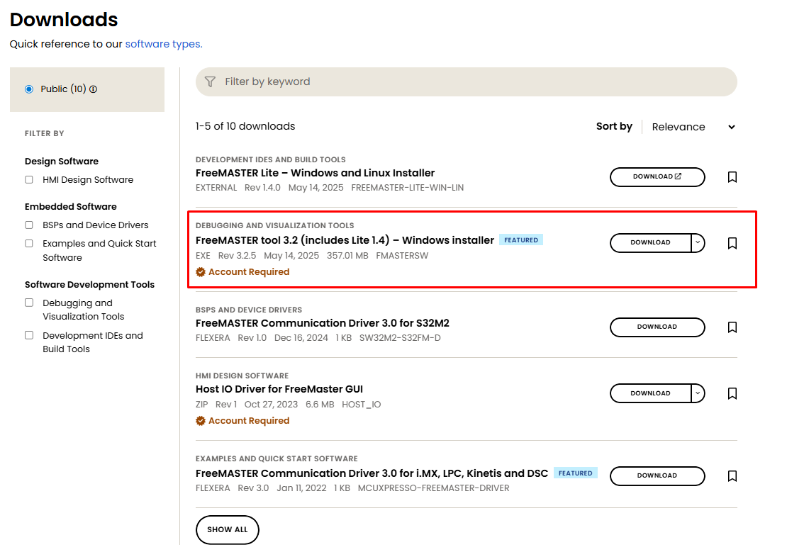
2.4 获取FreeMASTER运行时调试工具
S32K388EVB-Q289采用FreeMASTER运行时调试工具进行调试效果更好。
下载并安装FreeMASTER运行时调试工具
在S32DS中,从顶部菜单转到Help→S32DS Extensions and Updates(帮助→S32DS扩展和更新),打开“S32DS扩展和更新”对话框。
选择并安装FreeMASTER通信驱动程序。
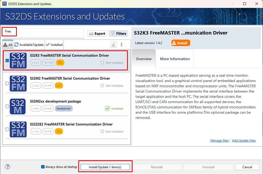
安装完成后,重启S32DS。
3. 连接
3.1 将跳线设置到默认状态
设置S32K388EVB-Q289评估板上的跳线。
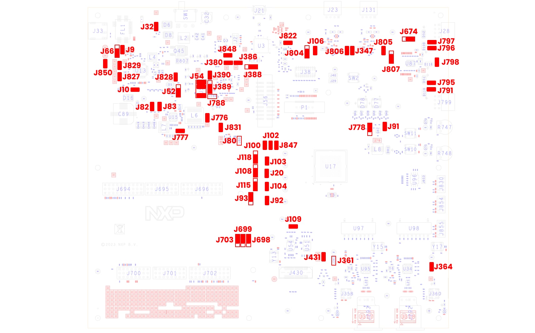
| 部件编号 | 封装说明 | 内部闪存 | RAM | EEPROM | |
|---|---|---|---|---|---|
| FS26/SBC电源 | J9 |
闭合 | FS26_WAKE2连接至RESET_MCU | ||
J10 |
闭合 | FS26 PGOOD信号已连接 | |||
J32 |
闭合 | VBAT连接至FS26接口和VSUP域 | |||
J52 |
1-2 | FS26调试选项选择 | |||
J54 |
1-2,5-6,7-8 | FS26 FCCU连接,连接VDD_HV_A_PERH和VDDIO信号,以及FS26_FCCU与FCCU MCU信号 | |||
J66 |
1-2 | FS26 WAKE1连接至MCU的PTA8 WKUP引脚 | |||
J827 |
闭合 | FS26_LDO1_OUT连接至VDD_HV_A. 5V输出 | |||
J828 |
闭合 | FS26_VCORE连接至V15 MCU 1.5V输出 | |||
J829 |
闭合 | FS26_LDO2_OUT连接至VDD_HV_B. 3.3V输出 | |||
J850 |
闭合 | FS26_VTRK1连接至FS26_P5V0 | |||
| PF5600 +3.3V输出 | J80 |
断开 | FS5600_I2C_SDA和FS5600_I2C_SCL信号 | ||
J82 |
闭合 | PF5600 EN1在上拉电阻后连接至VBAT_SW | |||
J83 |
闭合 | PF5600 EN2在上拉电阻后连接至VBAT_SW | |||
J776 |
闭合 | PF5600 P3V3SW_OUT1连接至多个3.3V接口,电压输出=3.3V | |||
J777 |
闭合 | PF5600 P3V3SW_OUT2连接至多个3.3V接口,电压输出=3.3V | |||
J831 |
闭合 | PF5600为I2C MCU信号提供电平转换,电源来自VDD_HV_A | |||
| PF5023 | J380 |
闭合 | PF50_SW1OUT_1V2启用1.2V输出 | ||
J386 |
闭合 | PF50_SW1OUT_1V8启用1.8V输出 | |||
J388 |
1-2 | PF5020 VDDIO_PWRAUX为PF5020 VIN选择P3V3SW_OUT1电源 | |||
J389 |
2-3 | PF5020输出通过上拉电阻启用电源 | |||
J390 |
闭合 | PF50_SW1OUT_1V1启用1.1V输出 | |||
J788 |
断开 | PF5020 RESET断开与RESET_MCU信号的连接 | |||
| S32K388 MCU电源 | J20 |
闭合 | V11 MCU连接。该跳线启用V11电源与MCU之间的连接 | ||
J91 |
闭合 | VDD_HV_DCDC启用DCDC转换器 | |||
J92 |
闭合 | 所选VDD_HV_B与VDD_HV_B_MCU之间的连接 | |||
J93 |
1-2 | 来自FS26_LDO2_OUT的VDD_HV_B电源 | |||
J100 |
闭合 | VDD_HV_A_PERH连接至VDD_HV_A | |||
J102 |
闭合 | VDD_HV_B_PERH连接至VDD_HV_B | |||
J103 |
闭合 | V15 MCU连接。该跳线启用V15电源与MCU之间的连接 | |||
J104 |
闭合 | 所选VDD_HV_A与VDD_HV_A_MCU之间的连接 | |||
J108 |
1-2 | V11/V15开关。为S332K388 MCU选择V11_MCU电压。V15选项仅用于与S32K358 MCU兼容。 | |||
J109 |
闭合 | 所选VDD_HV_A_MCU与VREFH_MCU之间的连接 | |||
J115 |
1-2 | 来自FS26_LDO1_OUT的VDD_HV_A电源 | |||
J118 |
1-2 | 来自FS26_VCORE的V15_MCU电源 | |||
J778 |
1-2 | 选择是否使用SMPS。如果不需要SMPS,则VDD_DCDC必须连接至VDD_HV_B_MCU | |||
J847 |
闭合 | VDD_REFH_PERH连接至VDD_HV_A | |||
| JTAG | J29 |
闭合 | 从VDD_HV_A_PERH到VDD_SWD/JTAG的电压供应,为JTAG接口供电 | ||
| 板载调试器 | J822 |
闭合 | 通过VDD_HV_A_PERH启用VDDIO_SDA的供电 | ||
J848 |
闭合 | 通过RESET_MCU信号启用SDA复位 | |||
| SABRE连接器 | J431 |
闭合 | 启用从P3V3SW_OUT1至SABRE连接器的供电 | ||
| GMAC0 TJA1120_A | J361 |
断开 | 启用P3V3_TJA1120_A的电源 | ||
| U97-1 | + | GMAC0引脚捆扎Config0 - pull-up | |||
| U97-2 | + | GMAC0引脚捆扎Config1 - pull-up | |||
| U97-3 | + | GMAC0引脚捆扎Config2 - pull-up | |||
| U97-4 | - | GMAC0引脚捆扎Config3 - pull-down | |||
| U97-5 | 0 | GMAC0引脚捆扎Config4 - open | |||
| U97-6 | + | GMAC0引脚捆扎Config5 - pull-up | |||
| U97-7 | 0 | GMAC0引脚捆扎Config6 - open | |||
| U97-8 | + | GMAC0引脚捆扎TJA1120_RST - pull-up | |||
| GMAC1 TJA1120_B | J364 |
闭合 | 启用P3V3_TJA1120_B的电源 | ||
| U98-1 | + | GMAC1引脚捆扎Config0 - pull-up | |||
| U98-2 | + | GMAC1引脚捆扎Config1 - pull-up | |||
| U98-3 | + | GMAC1引脚捆扎Config2 - pull-up | |||
| U98-4 | - | GMAC1引脚捆扎Config3 - pull-down | |||
| U98-5 | 0 | GMAC1引脚捆扎Config4 - open | |||
| U98-6 | + | GMAC1引脚捆扎Config5 - pull-up | |||
| U98-7 | + | GMAC1引脚捆扎Config6 - open | |||
| U98-8 | + | GMAC1引脚捆扎TJA1120_RST - pull-up | |||
| CAN0接口 | J106 |
闭合 | 启用从VBAT_SW到CAN0收发器的电源 | ||
J347 |
闭合 | 启用从P5V0SW_OUT1到CAN0收发器的5V电源 | |||
J804 |
2-3 | CAN0收发器VIO源自VDD_HV_B_PERH | |||
| CAN1接口 | J805 |
闭合 | 启用从P5V0SW_OUT1到CAN1收发器的5V电源 | ||
J806 |
闭合 | 启用从VBAT_SW到CAN1收发器的电源 | |||
J807 |
2-3 | CAN1收发器VIO源自VDD_HV_B_PERH | |||
| LIN接口 | J674 |
1-2 | LIN收发器VIO源自VDD_HV_B_PER | ||
J791 |
闭合 | LIN4 Commander*模式 | |||
J795 |
闭合 | LIN3 Commander*模式 | |||
J796 |
闭合 | LIN2 Commander*模式 | |||
J797 |
闭合 | LIN1 Commander*模式 | |||
J798 |
闭合 | TJA1124 LIN收发器的BAT电源 | |||
| ARDUINO连接器 | J698 |
1-2 | BEMF_C/PHC_I信号连接至PTE0引脚 | ||
J699 |
1-2 | BEMF_B/PHB_I信号连接至PTE1引脚 | |||
J703 |
1-2 | VDD_IO引脚连接至VDD_HV_A_PERH |
3.2 板上电
将SW1切换到OFF位置(完全向右),
连接12V电源适配器,将SW1开关置于ON位置(完全向左)。
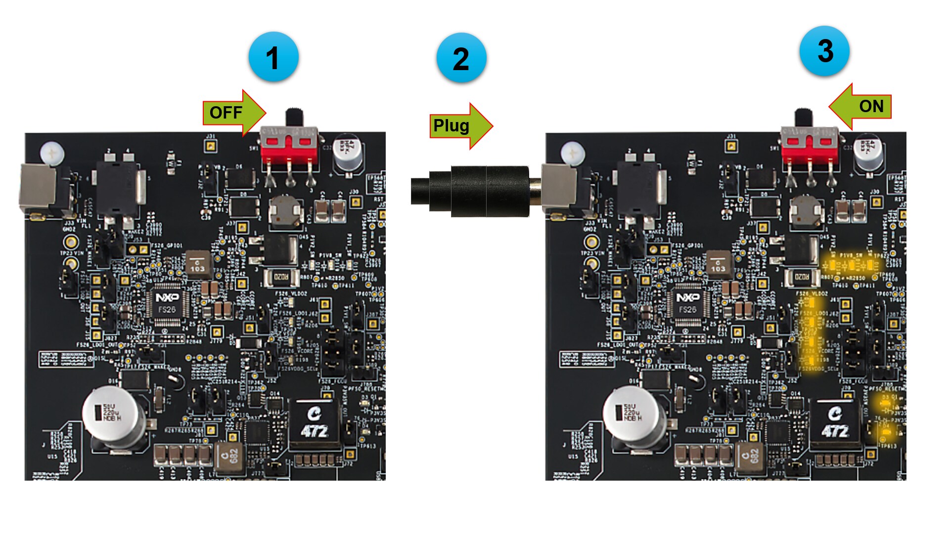
当EVB上电时,稳压器旁边的红色LED显示存在电源电压。
4. 构建和调试
立即试用S32K388EVB-Q289评估板。
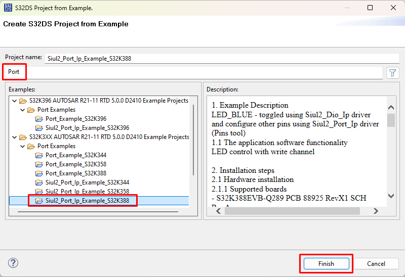
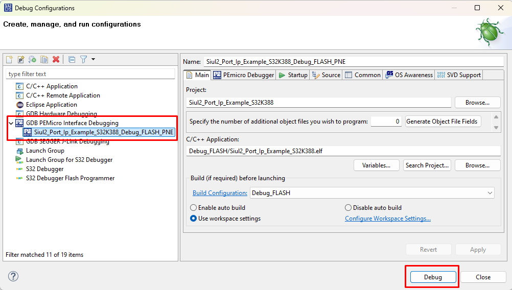
4.1 从示例创建S32DS项目
- 启动S32 Design Studio 3.6.2
- 前往menu→File→New→S32DS Project from Example (菜单→文件→新建→从示例创建S32DS项目)。选择一个RTD示例代码。例如Siul2_Port_Ip_Example_S32K388
4.2 生成配置
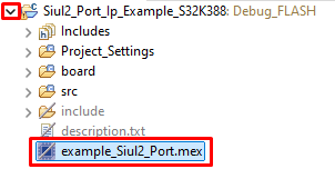
- 展开项目树,双击项目的mex文件
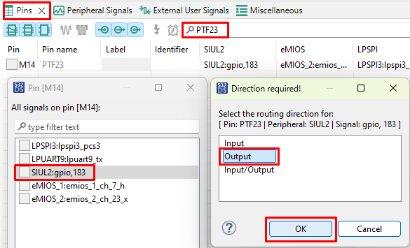
- 将
PTF23引脚(连接至绿色LED)设置为GPIO输出 - 定义
PTF23标识符(无空格)。例如""LED_G""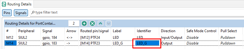
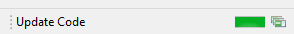
- 请确定配置了适当的项目,然后点击"Update Code"(“更新代码”)按钮生成配置文件

- 等待更新代码结束。在右下角查看状态
4.3 编辑代码
- 返回“C/C++”视图
- 双击src文件夹打开
main.c文件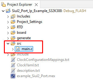
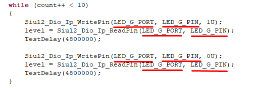
- 将"LED_PORT" (4个)和"LED_PIN" (4个)的所有实例修改为"LED_G_PORT"和"LED_G_PIN"。将红色LED更换为绿色LED
设计资源
支持
论坛
在我们的技术社区网站上,与其他工程师交流,并获得有关使用S32K388EVB-Q289评估板进行设计的专业建议。