TJA1410-EVB快速入门
上次修改时间:
Feb 16, 2026支持
TJA1410-EVB
本文档内容
-
开箱即用
-
硬件介绍
-
配置硬件
1. 开箱即用
恩智浦模拟产品开发板提供了一个易于使用的恩智浦产品评估平台。该板支持各种模拟、混合信号和电源解决方案。它们整合了单片集成电路系统级封装器件,采用成熟的高容量技术。恩智浦产品电池寿命长,设备尺寸小,组件数量少,成本低,性能高,帮助您打造先进的系统。本页面将指导您完成设置和使用TJA140-EVB板。
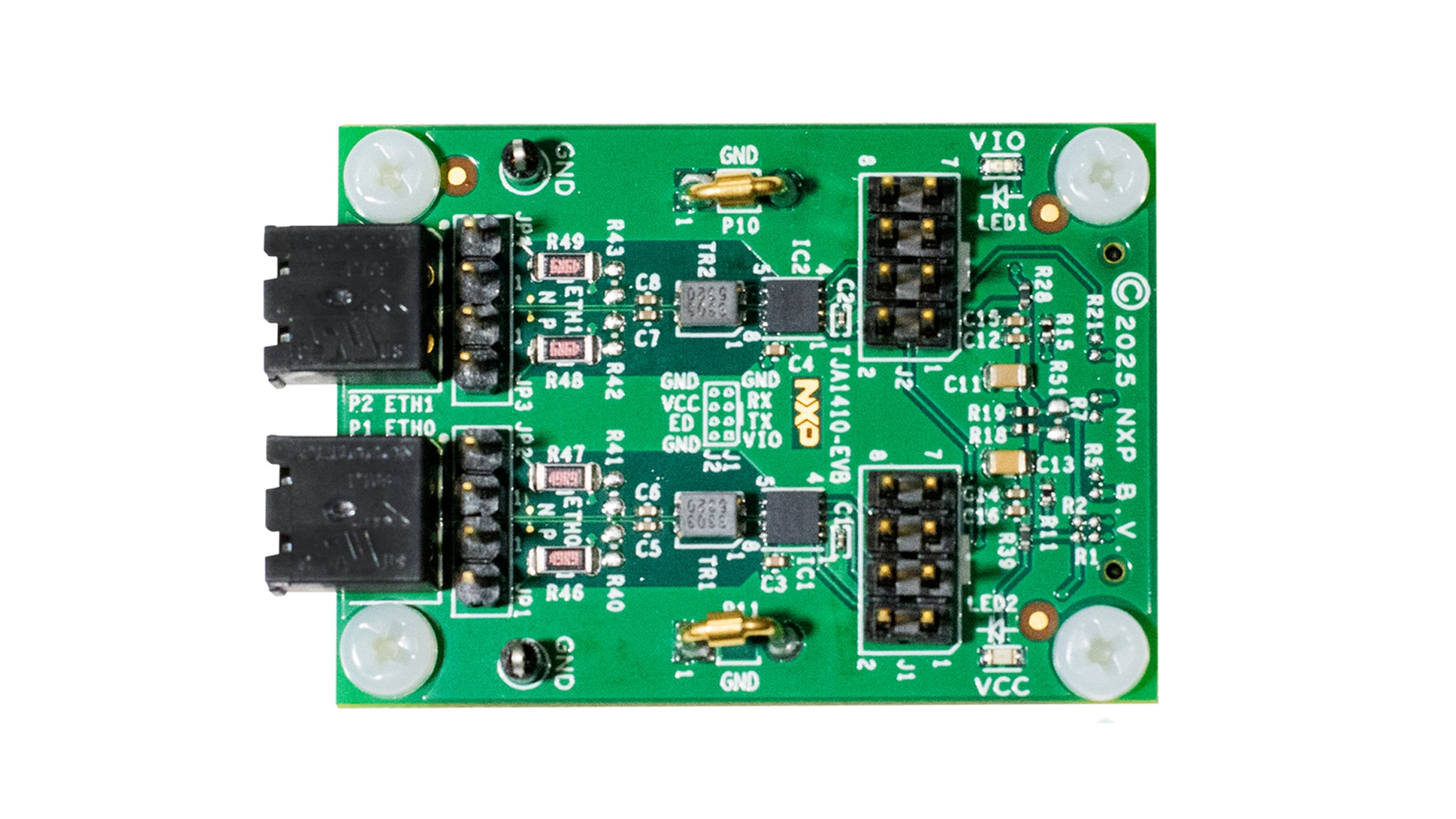
1.1 套件内含物
- TJA1410-EVB及两个插入式连接器,放在防静电袋中
1.2 其他硬件
- 要使用TJA1410-EVB进行10BASE-T1S应用的原型设计,需要一个配备集成数字物理层器件(PHY)的主机。主板选项:
- S32K5MMA-MB
- S32K566-EVB
- 电源:3.3V
- 根据连接器兼容性,可能需要使用带状线缆将TJA1410-EVB连接至主板
2. 硬件介绍
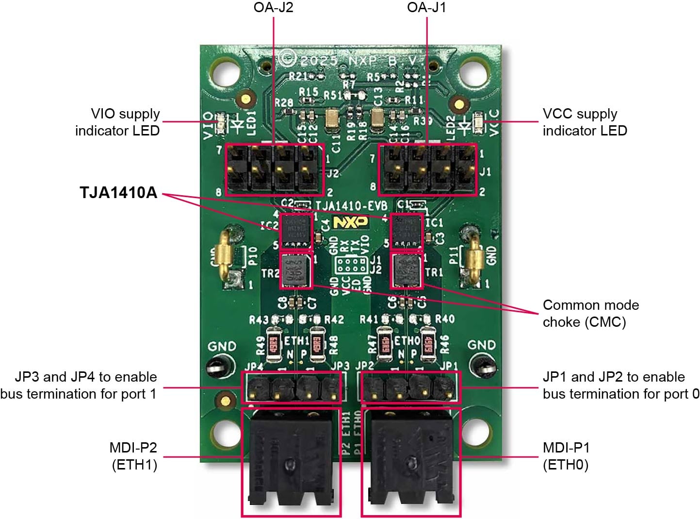
2.1 板特性
TJA1410-EVB集成了两个10BASE-T1S PMD收发器通道,每个通道包含:
- TJA1410A 10BASE-T1S以太网PMD收发器
- 终端节点端接跳线
- MDI连接器
- 两个OPEN Alliance PMD收发器接口连接器选项
- 电源LED指示灯
- 两个240μH共模扼流圈(CMC)
2.3 评估板推荐组件
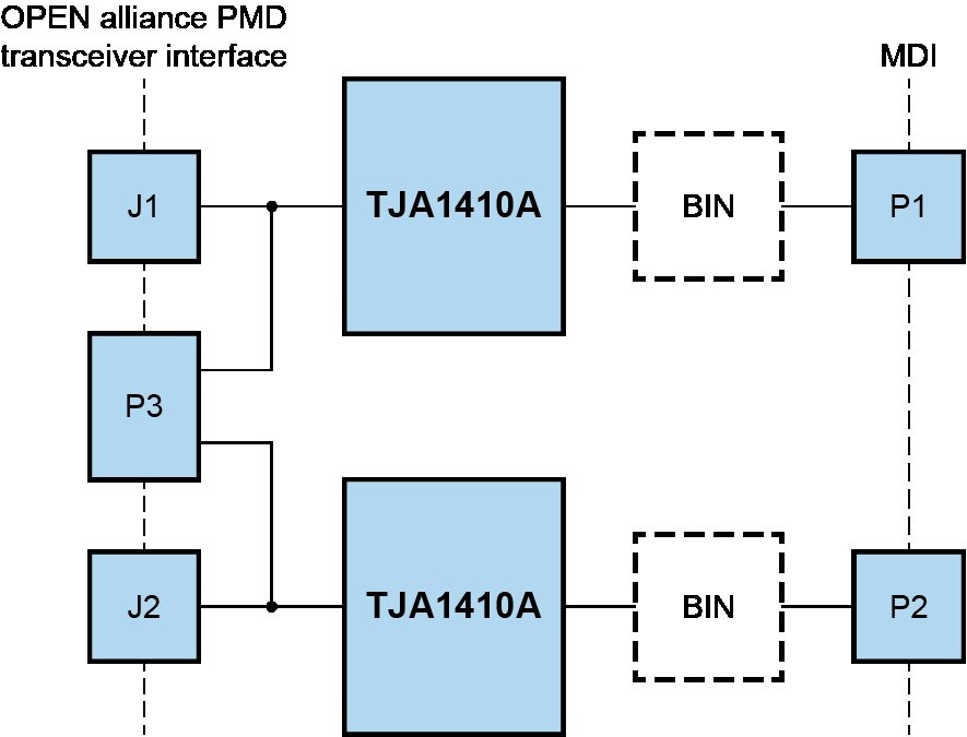
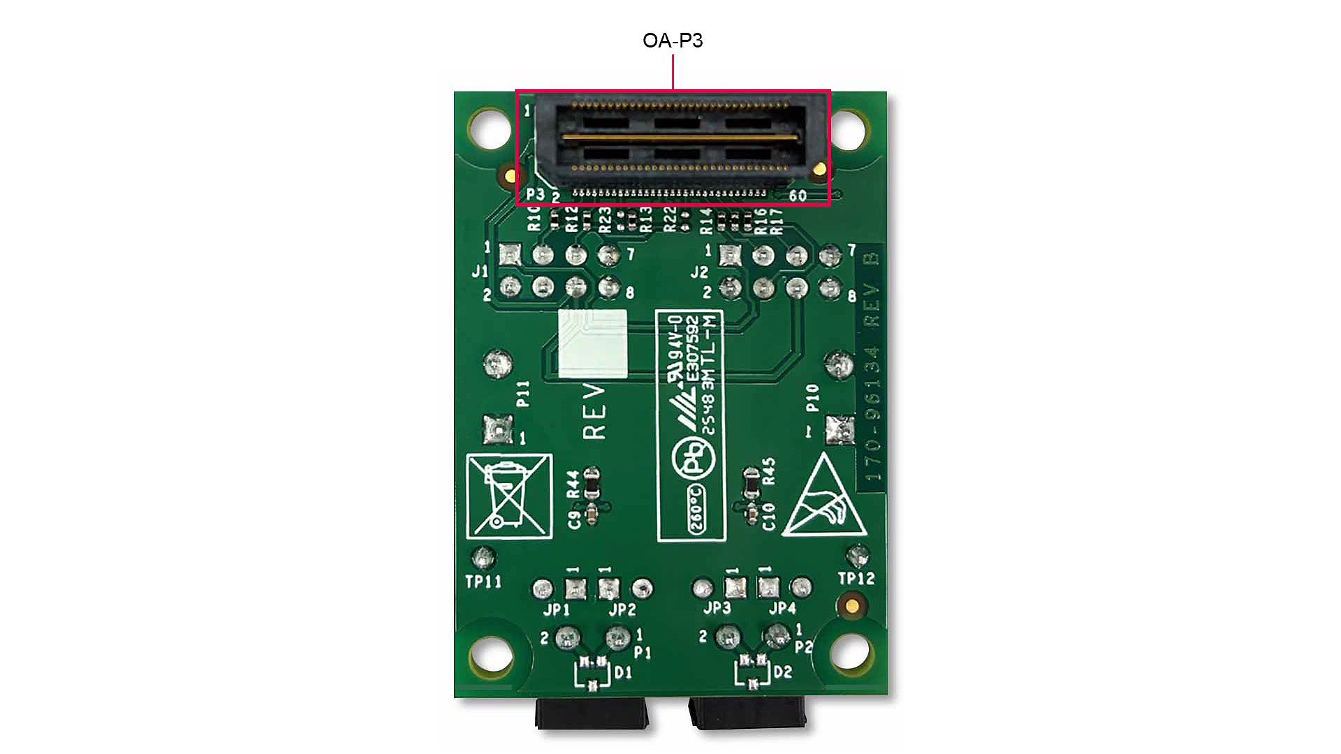
图2所示为TJA1410-EVB的概览及板上组件的位置。在图3所示的TJA1410-EVB的底面,可使用一个连接器(OA-P3)代替OA-J1和OA-J2。表1提供了这些组件的详细信息。
| 编号 | 说明 |
|---|---|
| OA-J1 | 端口1的OPEN Alliance 10BASE-T1S PMD收发器数字接口及电源连接器 |
| OA-J2 | 端口2的OPEN Alliance 10BASE-T1S PMD收发器数字接口及电源连接器 |
| OA-P3 | 端口1和端口2的OPEN Alliance 10BASE-T1S PMD收发器数字接口及电源连接器 |
VIO电源LED指示灯 |
VIO电源LED指示灯当VIO电源可用时会亮起 |
| VCC电源LED指示灯 | VCC电源LED指示灯当VCC电源可用时会亮起 |
| TJA1410A | 适用于3.3V VIO电源的OPEN Alliance 10BASE-T1S PMD收发器版本 |
| 共模扼流圈(CMC) | 符合OPEN Alliance 10BASE-T1S 共模扼流圈EMC测试规范的CMC |
端口0的JP1和JP2总线端接 |
跳线引脚为终端节点提供总线端接功能;JP1和JP2均需安装跳线插座,在端口0启用终端节点端接功能 |
端口1的JP3和JP4总线端接 |
跳线引脚为终端节点提供总线端接功能;JP3和JP4均需安装跳线插座,在端口1启用终端节点端接功能 |
| MDI-P1 | 端口1的介质相关接口 |
| MDI-P2 | 端口2的介质相关接口 |
2.4 EVB连接器
| 连接器引脚 | 信号 | 说明 |
|---|---|---|
| OA-Jx-1 | VIO |
TJA1410A的VIO接口供电电压;用于为数字I/O单元和唤醒检测电路供电 |
| OA-Jx-2、-7、-8 | GND |
接地 |
| OA-Jx-3 | TX_x |
TJA1410A发送数据信号 |
| OA-Jx-4 | ED_x |
TJA1410A能量检测信号 |
| OA-Jx-5 | RX_x |
TJA1410A接收数据信号 |
| OA-Jx-6 | VCC |
TJA1410A的收发器供电电压 |
| 连接器引脚 | 信号 | 说明 |
|---|---|---|
| OA-P3-28 | VCC |
TJA1410A的收发器供电电压 |
| OA-P3-30 | VIO |
TJA1410A的VIO接口供电电压;用于为数字I/O单元和唤醒检测电路供电 |
| OA-P3-6、-44 | GND |
接地 |
| OA-P3-4 | TX_0 |
TJA1410A端口0发送数据信号 |
| OA-P3-8 | RX_0 |
TJA1410A端口0接收数据信号 |
| OA-P3-16 | ED_0 |
TJA1410A端口0能量检测信号 |
| OA-P3-42 | TX_1 |
TJA1410A端口1发送数据信号 |
| OA-P3-46 | RX_1 |
TJA1410A端口1能量检测信号 |
| OA-P3-50 | ED_1 |
TJA1410A端口1接收数据信号 |
| OA-P3-1 | (VCC) |
通过0Ω电阻配置的备选VCC引脚分配选项(默认:未连接) |
| OA-P3-3 | (VIO) |
通过0Ω电阻配置的备选VIO引脚分配选项(默认:未连接) |
| OA-P3-11、-33 | (GND) |
通过0Ω电阻配置的备选GND引脚分配选项(默认:未连接) |
| OA-P3-16 | (TX_0) |
通过0Ω电阻配置的备选TX_0引脚分配选项(默认:未连接) |
| OA-P3-36 | (RX_0) |
通过0Ω电阻配置的备选RX_0引脚分配选项(默认:未连接) |
| OA-P3-43 | (ED_0) |
通过0Ω电阻配置的备选ED_0引脚分配选项(默认:未连接) |
| 连接器引脚 | 信号 | 说明 |
|---|---|---|
| MDI-Px-1 | BI_DAx_n | MDI连接器的负端 |
| MDI-Px-2 | BI_DAx_p | MDI连接器的正端 |
2.5 EVB跳线
| 跳线 | 配置 | 说明 |
|---|---|---|
JP1和JP2 |
断开 | 端口0分支节点端接 |
| 闭合 | 端口0终端节点端接 | |
JP3和JP4 |
断开 | 端口1分支节点端接 |
| 闭合 | 端口1终端节点端接 |
| LED | 状态 | 说明 |
|---|---|---|
VIO LED |
开 | VIO电源开启 |
| 关 | VIO电源关闭 |
|
VCC LED |
开 | VCC电源开启 |
| 关 | VCC电源关闭 |
3. 配置硬件
3.1 总线接口网络电路
图4展示了TJA1410 EVB的BIN电路。该电路遵循OPEN Alliance系统实施规范(参见参考文献5)。跳线JEP和JEN用于配置总线端接。表7列出并描述了BIN电路的组件。
TJA1410-EVB配备两个以太网端口。每个端口均包含一个相同的BIN电路。未安装的组件为可选组件,用于提供调整BIN电路的选项。
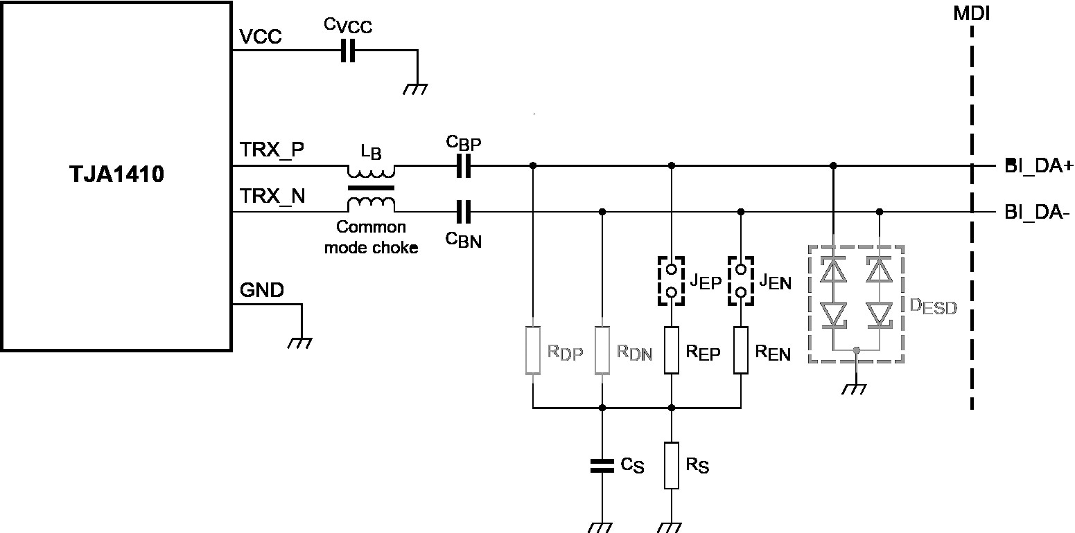
| 符号 | 原理图参考 | 值 | 说明 |
|---|---|---|---|
| LB | TR1、TR2 |
240µH | 符合参考文献4的典型CMC |
| CBP、CBN | C5、C6、C7、C8 |
100nF | 符合参考文献5的阻断电容 |
| JEP、JEN | JP1、JP2、JP3、JP4 |
— | 用于配置总线端接的跳线 |
| REP、REN | R46、R47、R48、R49 |
49.9Ω | 符合参考文献5的终端节点端接 |
| RDP、RDN | R40、R41、R42、R43 |
未安装(1.5kΩ) | 符合参考文献5的可选分支节点端接 |
| RS | R44、R45 |
100kΩ | 符合参考文献5的可选分体式滤波电阻 |
| CS | C9、C10 |
47nF | 符合参考文献5的可选分体式滤波电容 |
| DESD | D1 |
未安装 | 可选ESD保护器件 |
| CVCC | C3、C4 |
1µF | 用于缓冲VCC电源的多层陶瓷电容 |