UJA1023评估板快速入门
上次修改时间:
Mar 2, 2026支持
UJA1023-EVB
本文档内容
-
开箱即用
-
硬件介绍
1. 开箱即用
恩智浦的模拟产品开发板提供了一个易于使用的恩智浦产品评估平台。开发板支持各种模拟、混合信号和电源解决方案。它们采用成熟的高容量技术,整合了单片集成电路和系统级封装器件。恩智浦产品电池寿命长,设备尺寸小,组件数量少,成本低,性能高,帮助您打造先进的系统。
本页面将指导您完成设置和使用RD33774PC3EVB评估板。
使用UJA1023-EVB (UJA1023远程控制LIN I/O从设备)时,需要一块LIN主控制器板作为附加硬件。
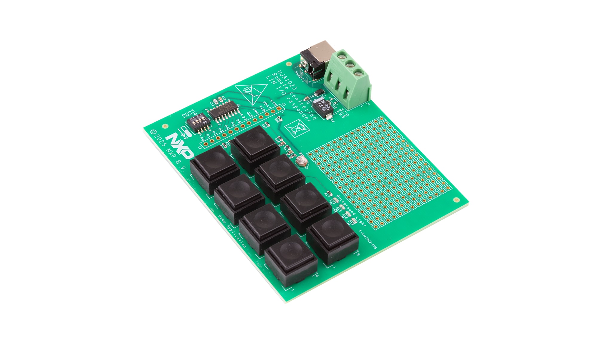
1.1 套件内含物
- UJA1023-EVB放在防静电袋中
- 快速入门指南
1.2 其他硬件
以下硬件是必需的,但未包含在本套件中:
- 12V电源
- LIN总线电缆
- LIN主控制器
- 以下为可选的LIN主控制器硬件选项:
- LIN接口工具
- S32K116EVB:S32K116-Q048汽车通用评估板
- S32K144EVB:S32K144-Q100汽车通用评估板
- S32K312MINI-EVB:S32K312MINI-EVB汽车通用评估板
- S32K3X4EVB-T172:S32K3X4EVB-T172汽车通用评估板
1.3 假设
用户需具备LIN诊断与配置规范的基础知识(参考2003年9月发布的LIN规范包2.0版本)。
2. 硬件介绍
2.1 板特性
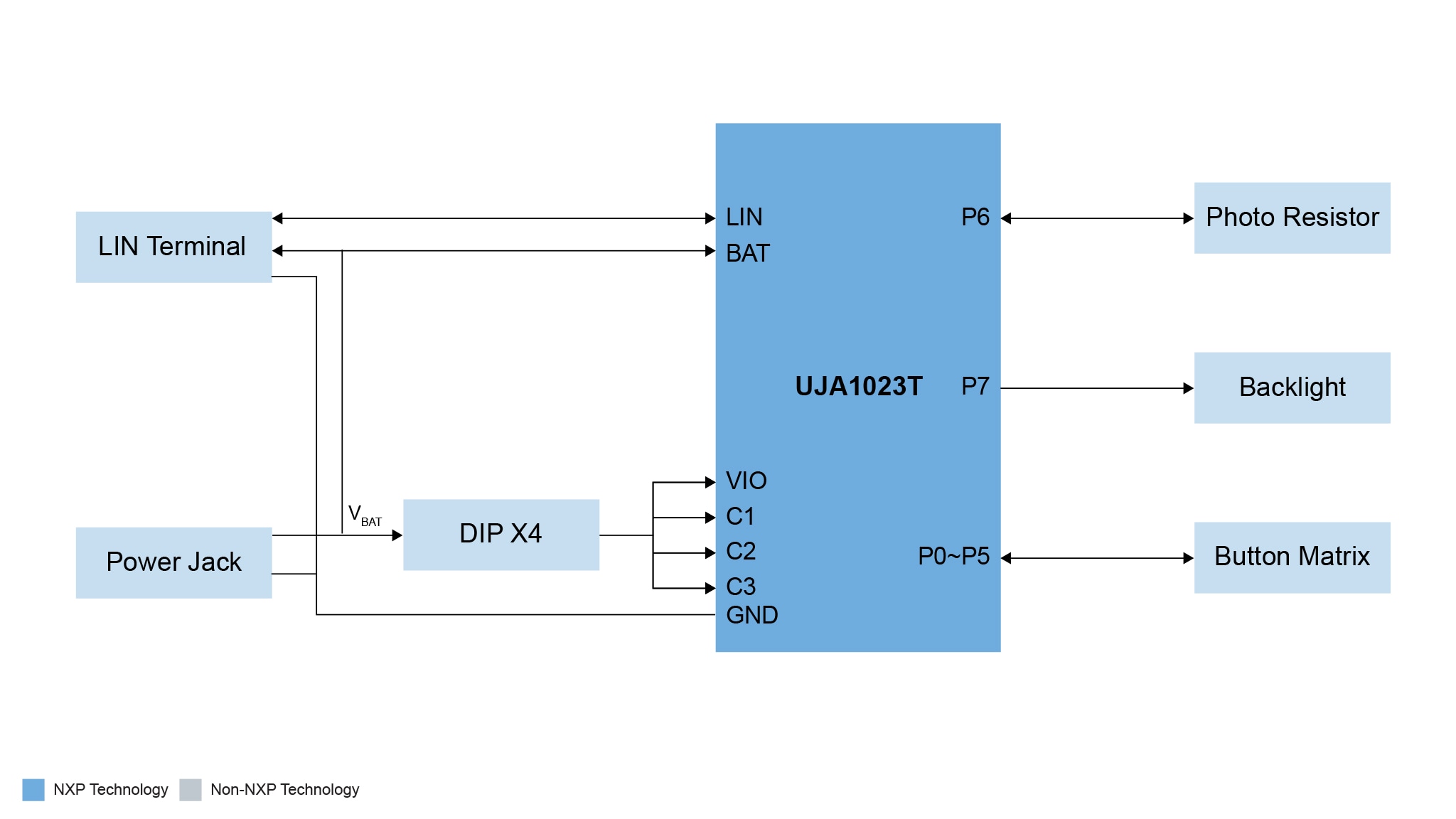
UJA1023-EVB评估板包含一个用户开关面板应用示例,其组成部分包括::
- UJA1023远程控制LIN I/O从设备IC
- 2x4开关矩阵(8个按钮)
- LED背光灯
- 光敏电阻传感器输入
- DIP开关,用于NAD配置
- 电源与总线连接器
2.3 EVB推荐组件
图2所示为UJA1023-EVB的概览及板上组件的位置。表1提供了这些组件的详细信息。
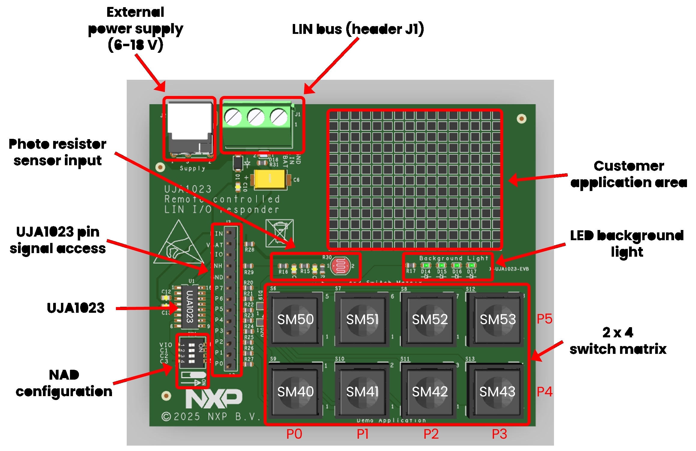
| 名称 | 说明 |
|---|---|
| 外部电源 | UJA1023-EVB的电源连接器 |
| LIN总线 | LIN总线连接器,含备用电源端子 |
| NAD配置 | DIP开关,用于LIN节点地址(NAD)配置以及VIO与VBAT的连接 |
| UJA1023 | 远程控制LIN I/O从设备IC:UJA1023 |
| UJA1023引脚信号访问 | 支持访问UJA1023引脚的连接器 |
| 2x4开关矩阵 | 带有8个按钮的开关面板应用电路 |
| LED背光灯 | 带有4个LED的背光灯应用 |
| 光敏电阻传感器输入 | 带有光敏电阻传感器输入信号的ADC应用电路 |
| 客户应用区域 | 用于进行应用原型设计的区域 |