FRDM-A-S32K118开发板快速入门
上次修改时间:
2026-07-29 12:13:00支持
FRDM-A-S32K118开发板
1. 开箱即用
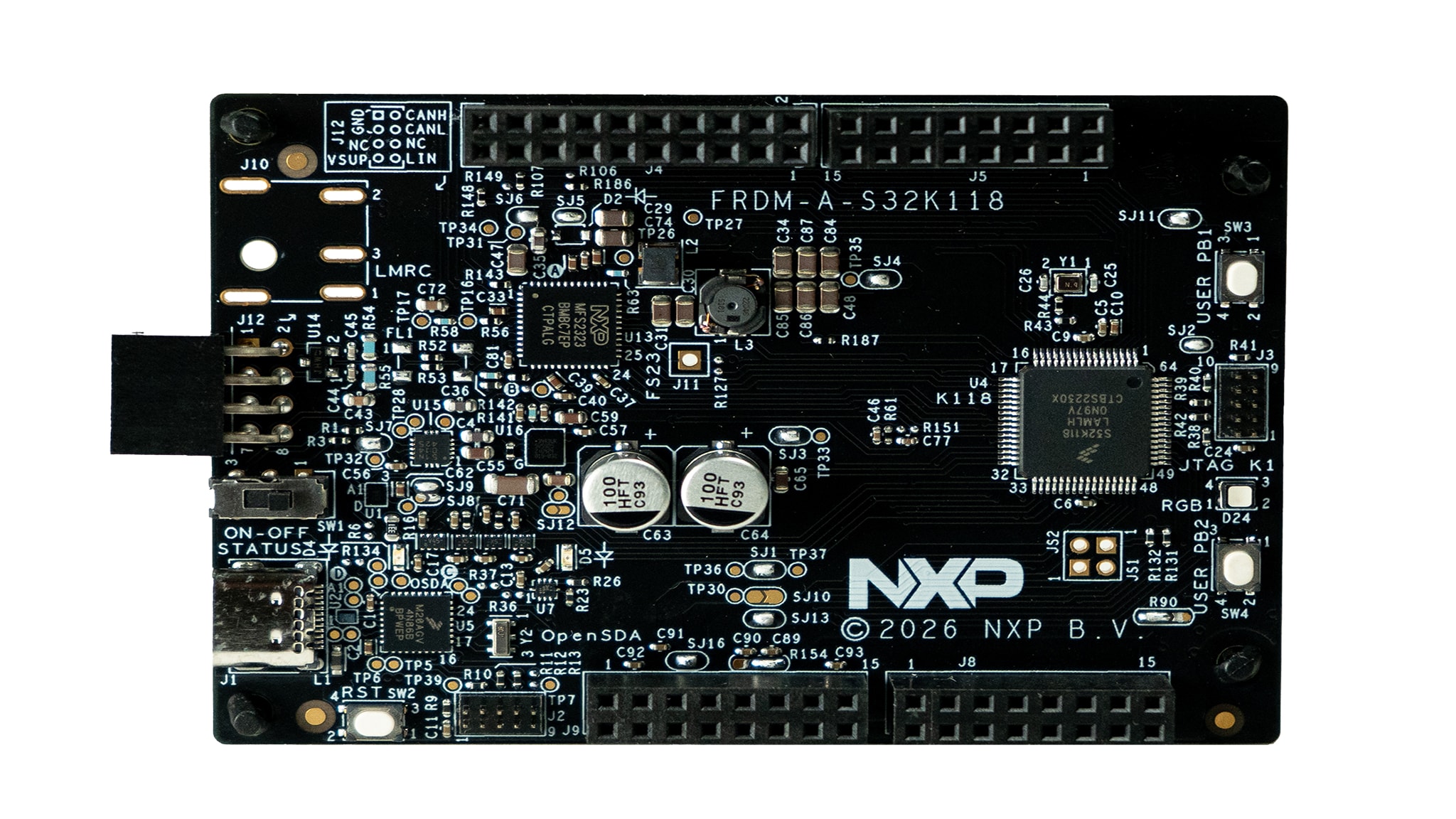
恩智浦FRDM-A-S32K118是一款高性价比开发板,旨在提供一个简洁而强大的平台,用于探索恩智浦S32K118车规级MCU的功能。FRDM-A-S32K118基于功能齐全的S32K118EVB-Q064,是汽车、嵌入式和工业系统工程师以及寻求紧凑型通用开发解决方案的业余爱好者的理想工具。
本指南将带您了解硬件组件和开发板配置。
1.1 套件内含物/装箱单
FRDM-A-S32K118内含物包括:
- FRDM-A-S32K118板
- USB Type-C线
- 快速入门指南卡
- 套件内含物清单
2. 获取软件
使用账号登录恩智浦官网。
2.1 安装软件
- 通过以下链接访问软件包:FRDM Automotive套件
- 点击“生成”进行下载
- 运行恩智浦Multi Installer
- 通过已创建的桌面快捷方式启动S32 Design Studio for S32 Platform 3.6.5
勾选"下载后启动可执行文件"(Launch executable after download)和"无需任何交互的安装与配置"(Installation and configuration without any interaction)选项后,FRDM软件包及其所有可用组件将被一并安装。
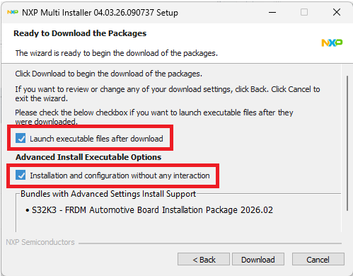
所有软件及工具将自动完成安装与配置。
2.获取硬件
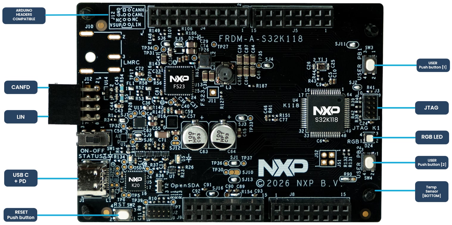
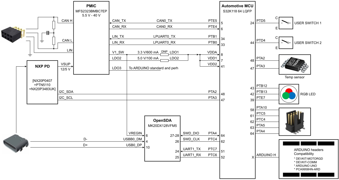
本节将带您了解FRDM-A-S32K118板的特性和组件。
3.1 板特性
- 供电相关器件:
- NX20P0407
- PTN5110
- NX20P3483UK
- 系统基础芯片(SBC) FS23
- 故障采集与控制单元(FCCU)安全引脚
- FS23上的嵌入式5Mb控制器局域网(CAN)
- 嵌入式本地互连网络(LIN)
- 基于Kinetis K20的OpenSDA调试接口
- S32K118汽车MCU,100 LQFP
- 10针、0.050英寸(1.27mm)表面贴装连接器接头,用于JTAG
- 两个用户按钮,用于调试
- RGB LED
- PCT2075D温度传感器
- 兼容以下接口的引脚:
- Arduino® UNO
- PCA9958HN-ARD
- DEVKIT-MOTORGD
- DEVKIT-COMM
3. 配置硬件
本节将指导您完成FRDM-A-S32K118板的设置。 配置详情请参阅随附的表格。
4.1 默认配置
| 接口 | 参考/信号 | 默认配置 | 注释 |
|---|---|---|---|
| 恩智浦供电 | U1 |
NX20P0407 | NX20P0407为配置通道(CC1/CC2)和边带使用(SBU1/SBU2)引脚提供智能过压保护,用于控制总线电压(VBUS)供电(PD),确保USB-C与外部电源之间安全高效的电源路径切换。 |
U15 |
PTN5110 | PTN5110用作USB PD物理层(PHY),管理USB Type-C通信,以协商电压和所需电流。 | |
U16 |
NX20P3483UK | NX20P3483UK用作USB Type-C应用的电源开关,为PO电路提供保护。 | |
USBC_I2C_SCL |
PTA3 | I²C时钟信号,用于从MCU (S32K118)向PHY (PTN5110)协商PO。 | |
USBC_I2C_SDA |
PTA2 | I²C数据信号,用于从MCU (S32K118)向PHY (PTN5110)协商PO。 | |
| FS23 | U13 |
MFS2323BMBA5EP | 此版本FS23除两个低压差稳压器(LDO)外,还包含一个DC-DC稳压器,为不同外设提供完备的电源管理。此外,该版本还集成了内部CAN和LIN PHY。 |
CANH |
J12-2 |
FS23提供的控制器局域网高电平(CANH)信号。 | |
CANL |
J12-4 |
FS23提供的控制器局域网低电平(CANH)信号。 | |
LIN |
J12-8 |
FS23提供的LIN信号。 | |
SJ4 |
• | FS23内置DC-DC转换器的5.0V输出电压。 | |
SJ6 |
• | FS23 LDO2的3.3V输出电压。 | |
SJ7 |
• | FS23 LDO3的5.0V输出电压。 | |
| OpenSDA | U5 |
MK20DX128VFM5 | 连接至S32K118的板载调试接口。 |
| MCU | U4 |
S32K118 | ASIL B级单Arm® Cortex®-M4 MCU,主频80MHz (HS-RUN模式下为112MHz),配备2MB通用闪存。 |
| JTAG | J3 |
• | S32K118 MCU的JTAG接口通过10引脚1.27mm接头连接。 |
| 用户RGB LED | D24 |
PTB12——FTM0_CH0 | 蓝色高电平有效。 |
- |
PTB13——FTM0_CH1 | 绿色高电平有效。 | |
- |
PTE7——FTM0_CH7 | 红色高电平有效。 | |
| 用户按钮 | SW3 |
PTD5 | 用于一般用途。 |
SW4 |
PTD4 | 用于一般用途。 | |
| 温度传感器 | U18 |
PCT2075D | I²C温度-数字转换器,在-25°C至+100°C范围内精度为±1°C。引脚兼容LM75。 |
4.2 焊桥跳线配置
| 接口 | 参考/信号 | 默认配置 | 注释 |
|---|---|---|---|
| 供电 | SJ3 |
• | 用于将电源开关(U16)的输出连接至FS23输入的焊桥。 |
SJ8 |
• | 用于为USB Type-C端口保护电路供电的焊桥。 | |
SJ9 |
- | 未焊接的辅助焊桥,用于为USB Type-C端口保护电路供电。 | |
SJ12 |
- | 未焊接的焊桥,用于为电源开关USB Type-C的5.5V引脚供电。 | |
| FS23 | R45 |
1-2 | 用作选择器的焊桥,用于选择USB Type-C供电还是电源插孔供电。 |
SJ4 |
• | 用于将PMIC的DC-DC降压输出连接至整个板电源的焊桥。输出电压为5V。 | |
SJ5 |
• | 用于旁路FS23 LDO2输出(无二极管保护)的焊桥。 | |
SJ6 |
• | 用于将PMIC LDO2输出连接至板电源的焊桥。输出电压为3.3V。 | |
SJ7 |
• | 用于将PMIC LDO3输出连接至板电源的焊桥。输出电压为3.3V。 | |
| OpenSDA | SJ15 |
• | 用于选择MK20输入电压(来自FS23 V1输出)的焊桥。 |
SJ14 |
- | 用于选择MK20输入电压(来自FS23 V3输出)的焊桥。 | |
SJ1 |
• | 用于将MCU VDD电源连接至电压转换器的焊桥,该转换器用于将板载调试器MK20的信号传输至S32K1。 | |
| MCU | SJ10 |
• | 用于将PMIC V1输出电压连接至S32K1的焊桥。 |
SJ13 |
- | 用于将PMIC V2输出电压连接至S32K1的焊桥。 | |
| JTAG | SJ2 |
• | 用于为JTAG连接器供电的焊桥。 |
| Arduino | R153 |
1-3 | 焊桥选择器,用于选择从PMIC至Arduino连接器的3.3V基准的参考电压。 |
R154 |
1-3 | 焊桥选择器,用于选择从PMIC至Arduino连接器的5.0V基准的参考电压。 | |
SJ1 |
• | 用于将PTA2连接至J5-3,或通过JS2外接1x2接头(HDR),将PTA2连接至J5-1的焊接跳线。 |
|
SJ2 |
• | 用于将PTA3连接至J5-1,或通过JS2外接1x2 HDR,将PTA3连接至J5-3的焊接跳线。 |
|
| 用户外设 | SJ11 |
• | 用于使能板外设部分的焊桥。 |
R90 |
1-3 | 用于选择3.3V或5V为RGB LED供电的焊桥。 |
设计资源
支持
培训
论坛
访问恩智浦的技术社区网站,与其他工程师交流,获取如何使用FRDM-A-S32K118开发板进行产品设计的专业建议。