设计文件
1 设计文件
-
符号和尺寸
PCA9615DP-TSSOP10-CAD Symbol and PCB Footprint – BXL File
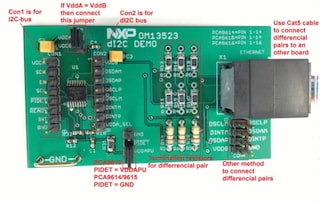
The PCA9615 is a Fast-mode Plus (Fm+) SMBus/I²C-bus buffer that extends the normal single-ended SMBus/I²C-bus through electrically noisy environments using a differential SMBus/I²C-bus (dI²C) physical layer, which is transparent to the SMBus/I²C-bus protocol layer. It consists of two single-ended to differential driver channels for the SCL (serial clock) and SDA (serial data).
The use of differential transmission lines between identical dI²C bus buffers removes electrical noise and common-mode offsets that are present when signal lines must pass between different voltage domains, are bundled with hostile signals, or run adjacent to electrical noise sources, such as high energy power supplies and electric motors.
The SMBus/I²C-bus was conceived as a simple slow speed digital link for short runs, typically on a single PCB or between adjacent PCBs with a common ground connection. Applications that extend the bus length or run long cables require careful design to preserve noise margin and reject interference.
The dI²C-bus buffers were designed to solve these problems and are ideally suited for rugged high noise environments and/or longer cable applications, allow multiple followers, and operate at bus speeds up to 1 MHz clock rate. Cables can be extended to at least 3 meters (3 m), or longer cable runs at lower clock speeds. The dI²C-bus buffers are compatible with existing SMBus/I²C-bus devices and can drive Standard, Fast-mode, and Fast-mode Plus devices on the single-ended side.
Signal direction is automatic, and requires no external control. To prevent bus latch up, the standard SMBus/I²C-bus side of the bus buffer, the PCA9615 employs static offset, care should be taken when connecting these to other SMBus/I²C-bus buffers that may not operate with offset.
This device is a bridge between the normal 2-wire single-ended wired-OR SMBus/I²C-bus and the 4-wire dI²C-bus.
Additional circuitry allows the PCA9615 to be used for ‘hot swap’ applications, where systems are always on, but require insertion or removal of modules or cards without disruption to existing signals.
The PCA9615 has two supply voltages, VDD(A) and VDD(B). VDD(A), the card side supply, only serves as a reference and ranges from 2.3 V to 5.5 V. VDD(B), the line side supply, serves as the majority supply for circuitry and ranges from 3.0 V to 5.5 V.
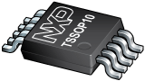
部件编号包含: PCA9615DP.
1 设计文件
如需恩智浦直接支持,请参阅 工程服务.
2 工程服务

查找支持此产品的所有合作伙伴,请参阅 合作伙伴市场.